This thread has been locked.

If you have a related question, please click the "Ask a related question" button in the top right corner. The newly created question will be automatically linked to this question.

ADS8900B: pspice model

Part Number: ADS8900B

Hi team,

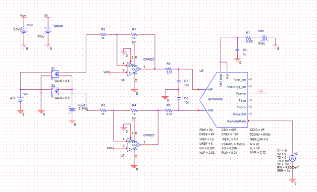
One of our customer is experiencing some parameters that are not understood when using the pspice model simulation, could you please help explain:

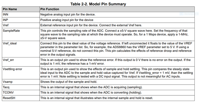
Which pin of the digital output of this chip is Vsamp?

Why can't I get digital waveforms when I do time domain analysis? How can I save a digital waveform?

What does Tacq、Tconv、ResetSH mean?
Best Regards,

Amy Luo

  • Hello Amy,

    The ADS8900B PSPICE model only models the analog portion of the ADC, including the sample and hold front-end of the ADC.  The purpose of the model is to properly design the ADC input amplifier and reference to insure proper settling during the acquisition phase of the conversion cycle.  The model does not provide a digital output word that is the equivalent of the input voltage.

    The following application note describes the model in detail and how to use it in a simulation.

    Understanding and Using SAR ADC SPICE Micromodel

    Each of the pins are described in Table 2 of the application note and copied below for reference.

    The primary output signal of interest is the Vsettling_error, which shows the settling time for the ADC.  This output should settle as close to 0 error within the ADCs acquisition period.  When operating the ADS8900B at 1MSPS, the total acquisition time is 300nsec.

    Regards,
    Keith Nicholas
    Precision ADC Applications

  • Hi Keith,

    Thank you for your assistance.

    Best Regards,

    Amy