This thread has been locked.

If you have a related question, please click the "Ask a related question" button in the top right corner. The newly created question will be automatically linked to this question.

ADS1120: It was supposed to receive the three data of 05, 42, 80, but received it was 0XFF high. What is the reason for this? Document: ads1120.txt

Part Number: ADS1120
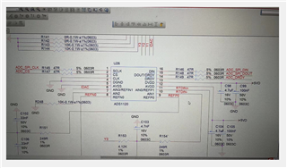
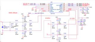
Other Parts Discussed in Thread: ADS1220

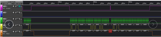
The software sends commands 0X23 read registers, and the data is received all the 0XFF.  It was supposed to receive the three data of 05, 42, 80, but received it was 0XFF high.  What is the reason for this?

static int Dev_ads1120_Config(void)
{
	struct ADS1120_REGS regs;
	
	memset(&regs, 0, sizeof(regs));
	
	/* 系统复位 */
	Dev_ads1120_Reset();

	regs.R0.PGA_BYPASS = 0x0;	//0: PGA enabled (fault) 			1: PGA disenabled and bypassed
	regs.R0.GAIN = 0x0;			//0: Gain = 1 (default)
	regs.R0.MUX = 0x0;			//0: AINP = AIN0, AINN = AIN1 (default)
	
	regs.R1.DR = 0x0;			//0: 20 SPS
	regs.R1.MODE = 0x0;		//0: Normal Mode (256kHz default)
	regs.R1.CM = 0x1;			//0: Signal-shot mode (default) 	1: Continuous conversion mode
	regs.R1.TS = 0x0;			//0: Disable temperature sensor		1: Enable temperature sensor
	regs.R1.BCS = 0x1;			//0: Current sources off (derfault)	1: Current sources open
	
	regs.R2.VREF = 0x1;			//1: External reference selected using dedicated REFP0 and REFN0 inputs
	regs.R2.RES_5060 = 0x0;
	regs.R2.PSW = 0x0;
	regs.R2.IDAC = 2;			//0: OFF(default)
	
	regs.R3.I1MUX = 0X4;		//0: IDAC1 disabled (default)
	regs.R3.I2MUX = 0x0;		//0: IDAC2 disabled (default)
	regs.R3.DRDYM = 0x0;
	regs.R3.RES_0 = 0x0;
	
	Dev_ads1120_WriteReg(ADDR_REG_0, (uint8_t *)&regs, 4);
	memset(&regs, 0, sizeof(regs));
	Dev_ads1120_ReadReg(ADDR_REG_0, (uint8_t *)&regs, 4);
	return 0;
}

static int Dev_ads1120_WriteReg(uint8_t addr, uint8_t *buf, uint8_t lens)
{
	uint8_t cmd[5] = {0};
	
	cmd[0] = CMD_WREG | (addr << 2) | (lens - 1);
	memcpy(cmd + 1, buf, lens);
	
	Spi_SetCS(M0P_SPI0, FALSE);
	Spi_SendBuf(M0P_SPI0, cmd, lens + 1);
	delay1us(1);
	Spi_SetCS(M0P_SPI0, TRUE);
	
	return 0;
}
static int Dev_ads1120_ReadReg(uint8_t addr, uint8_t *buf, uint8_t lens)
{
	uint8_t cmd[4] = {0};
	
	cmd[0] = CMD_RREG | (addr << 2) | (lens - 1);

	Spi_SetCS(M0P_SPI0, FALSE);
	Spi_SendData(M0P_SPI0, cmd[0]);
	Spi_ReceiveBuf(M0P_SPI0, buf, lens);
	delay1us(1);
	Spi_SetCS(M0P_SPI0, TRUE);
	
	return 0;
}

static int Dev_ads1120_Reset(void)
{
	uint8_t cmd[2] = {CMD_RESET};

	Spi_SetCS(M0P_SPI0, FALSE);
	Spi_SendBuf(M0P_SPI0, cmd, 1);
	Spi_SetCS(M0P_SPI0, TRUE);
	delay1us(100);
	return 0;
}

  • Aiwen,

    Thanks for sending the logic analyzer output.  This is more helpful than code for debugging the issue.   

    1.  You mention sending command 0x23 then expecting to read 3 registers.  This is the correct command to read 3 registers starting at register 0x00.  So I agree with your approach.

    2.  Looking at the logic analyzer output.  I see that you send 0x06.  This is the command for RESET.  Can you double check that you are capturing the correct information?  If you are capturing the correct information, can you change the write to 0x23.

    Best regards,

    Art

  • Hi  Art;

    1、today,We have chage another one ADS1120, At first, it was normal, and after working for a while, the state began to appear abnormal, the same as the previous problem. I wonder if this is a software issue or a hardware issue?

    2、I don't understand what you said earlier that you say change the write to 0x23.Could  you please explain it a  little more detail?

    1. This is an indication that the device was damaged.  Since the new device also eventually failed, this is an indication that you have an issue that will overstress the device and damage it inherent in your system.  Since the device always outputs FF it is possible that the digital output was damaged.  It is also possible that the entire device is damaged and non-functional.  Exceeding any of the absolute maximum specifications could cause this to happen.  I would start by checking the supply voltages during power up.  Also, is DVDD at the same level as your digital communications?  Turning on any analog input signal or digital signal before the supplies (AVDD and DVDD) are active can damage the device. 
    2.   Table 14 lists all the commands for ADS1120.  The command byte for RESET is 0000 011x (where x is don't care).  Looking at your logic analyzer output this is the command that was sent.  The command for RDATA is 0x23.  This is what you told me you sent.  This would be the correct command to send for reading registers, but this is not what is displayed in your logic analyzer picture.
    3. I do not see anything unusual in your schematic.  You will have to look at all the pins with a scope to understand where the overstress signal is coming from.  If you change the device again and it works but eventually fails this would be a very strong indication that you have an issue with overstress.

    Thanks for your updated information.  Once you understand the source of the overstress, we can look at ways to eliminate it.  I agree with your point that this is not a software issue, but seems to be a hardware problem.

    Art

  • Hi  Art;

    Thanks  for  your reply, in addition,I have other questions。Will the configuration of this chip cause the current to be output from AIN0 or AIN1? The currently configured AIN3 output current, but I measured 0.01mA from the AIN0 side, is this normal?

  • Aiwen,

    Unless a channel is configured to output an IDAC current, the current on the analog inputs should be limited to nano-amps.  Damaging an input from overstress can cause a leakage.  Also, you need to make sure that your meter is capable of accurately reading any current you measure.  Also, solder flux residue can cause leakage paths if the PCB is not cleaned properly.

    Art

  • Hi  Art:

    I use this combination with the matrix switch to collect the temperature of the 8-way sensor, I directly disconnect the matrix switch, directly connected to one of my sensors, and the chip is replaced with ADS1220, Or is there the same phenomenon as ADS1120 (there is a voltage of 0.025V across the platinum resistor, and the voltage at the acquisition terminal is 0.123V), I remove the resistor R154 and R158 after the right end voltage of R153 and R157 is the same as the left end voltage of 0.025V, welding R154 and R158, R153 and R157 left terminal voltage is 0.025V, right terminal voltage is 0.123V, want to ask whether AIN0 and AIN1 itself have a certain voltage difference, there will be leakage current? The MCU is successful in controlling the ADC。

    So ,could you please help to check it?why Why is this happening?How to  solve it?

  • Aiwen,

    1. In your design I do not see any obvious path for the IDAC current to flow into the RTD.  Are you using one of the configurations shown in the data sheet for RTD measurement?  If so, which one?  I suggest you review https://www.ti.com/lit/an/sbaa275/sbaa275.pdf.  This document covers RTDs and the standard configurations in detail.
    2. To directly answer your question, I do not follow your debug method.  The image shows one voltage on terminals Y3 and Y2 and a different voltage on the ADC input.  Is the IDAC configured to flow through the filter network?  Is the IDAC on during the measurements?
    3. I think the key to understanding the issue is to confirm how the IDAC is applied to the RTD. 

    Best regards, Art