


Other Parts Discussed in Thread: ADC32RF42, LMK04828
Hello,
we have been debugging ADC32RF42 for nearly a year, but there is still some confusion. I look forward to your help.
We used ADC32RF42 and LMK04828 chips. Currently, the bypass mode failed to build a link. But the DDC pattern can establish links.
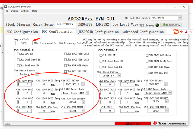
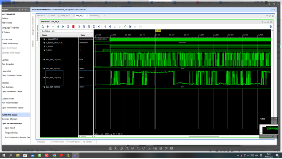
DDC mode uses the dual passband complex 4841 mode, the clock module should have no problems, the download is also the official program. At present, the 1GSPS with sampling rate can normally receive data under the link layer transmission layer and 12bit test mode. However, in the test mode 0/1 of DDC, the data could not be received, and the FPGA end could only see half of the chaotic data when the oscilloscope gave the signal. I don't know what the problem is. DDC configuration interface diagram and vivado upper board diagram are as follows:
Best regards
Kailyn
