This thread has been locked.

If you have a related question, please click the "Ask a related question" button in the top right corner. The newly created question will be automatically linked to this question.

ADS1178: Problems interpreting Data

Part Number: ADS1178

Dear all,

I did an aprentice project in my company and have some trouble with getting data out of my ads1178. I use the SPI interface in TDM Fixed position and an Arduino MEGA2560 to bitbang the spi interface. Vref is 2.5 V and Vcc is 5 V. I use all channels and clock the ADC at 250 kHz as I do not need a high data rate.

The Problem is as following. I Measure 2.49 V at the differential inputs. As per my Understanding, the ADC should be capable of measuring up to 5 V at its differential pins. The Scope shows a bit value of around 1120DEC with an differential input Voltage of 2.45 V. That would leave no Headroom for a higher Voltage than, say, 2.5 V. My Arduino interface also gives me the bitmask my Scope is showing so I assume its working as intended so I am missing something.

Arduino Code


The following code does the bitbanging:


void DataRead()
{

  for (int n = 0; n < 128; n++)//Runs loop 128 times to catch 128 bit
  {
 
    digitalWrite(52, HIGH);//Set SCKL to high
    delayMicroseconds(25);   //Wait 25uS      
    digitalWrite(52, LOW);//Set SCKL to low, data is shifted out afterwards by ADC
    //delayMicroseconds(5); //Wait 5 uS
    DataBits[n] = digitalRead(50); //Read Dout pin of ADC and write in to an bool array
    
    delayMicroseconds(15);//Wait til SCKL is put high again
  }

I then calculate the voltage from the DEC vals to Voltages as per:

Voltage = DecVal * LSB; // Conversation to Voltage with LSB= 2.5 V / 2^15
Voltage = Uref-Voltage;// Setting the Value in Relation to Uref, Uref=2.5 V

And those are not making any sense. I expect a DEC Value of around 16 kDEC (Half input Range of 5 V total with 2.5 V input with 32 kDEC range) but I am getting more around 1100DEC, on the Scope as well as in Code. I am running out of Ideas and would like to ask if someone has Experience with this ADC one could share or sees an mistake I may have made in my Schematic/Code. I think I misunderstood something but I cant put my finger on it for the life of me.


Schematic of ADC:


I hope they are readable, thanks in Advance for taking Time on this!

  • Hello Christian,

    Welcome to the TI E2E community.

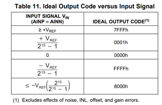
    The full scale input range of the ADS1178 is +/-Vref (differential).  The AINPx and AINNx pins can range from 0V to 5V (measured relative to the AGND pin), but the maximum differential voltage with Vref=2.5V is +/-2.5V.

    For example, if you connect the AINNx to +2.5V, then the AINPx pin can range from 0V to 5V.

    AINP=0V, AINN=2.5V, Vdiff=(AINP-AINN)=(0-2.5)=-2.5V, negative full scale output code 8000h

    AINP=2.5V, AINN=2.5V, Vdiff=(AINP-AINN)=(2.5-2.5)=0V, 0000h

    AINP=5V, AINN=2.5V, Vdiff=(AINP-AINN)=(5-2.5)=+2.5V, positive full scale output code 7FFFh

    The output code is two's compliment (signed integer).  Your calculation for LSB is correct; LSB= 2.5 V / 2^15.

    Also, looking at your code, you are not reading the data out of the ADS1178 fast enough.  With CLK=8MHz, the output data rate will be 3125sps, or a data rate period of 320µsec.  The data must be shifted out in a time period less than 320µsec.  Based on your code, SCLK period is about 50µsec, which only leaves enough time to shift out the first 6 bits of the 128b SPI frame.  If you do not want to increase SCLK frequency, then reduce the CLK frequency to less than 400kHz (minimum CLK frequency is 100kHz).

    Regards,
    Keith Nicholas
    Precision ADC Applications

  • Hi Keith,

    thanks for your detaild reply! It did clearify some things. The Clock rate in my Schematic is a typo and is currently at 250 kHz. I made some improvised changes to my PCB. AINP is now fixed to 2.5 V and AINN ranges from 0 V to 5 V. But I still get the Bit Values mentioned in my first post which seem incorrect with an input Voltage of 1.2 V at AINN. Did I still miss something?

    Greetings, Chris

  • Hello Chris,

    The data can be corrupted if not read before the next /DRDY high to low transition.  It is not clear from your code if you are monitoring the /DRDY output, and then clocking data after /DRDY asserts low and completing the transfer before the following /DRDY assert low.

    Also, if the power supply sequence is not followed in Figure 24 of the datasheet, the device may not be reset properly and you can get inconsistent operation.  The start-up sequence in figure 24 is not necessary if you assert the /SYNC pin after power-up, since the assertion of /SYNC will also force a reset of the device.

    First confirm if you are reading the data at the proper time between /DRDY assertions.  If this timing is correct, then you may have a power-up issue, requiring either the assertion of the /SYNC pin or changes to your power supply section to meet figure 24 requirements.

    Please send a scope or logic capture of the /DRDY, SCLK, and DOUT pins for a full frame and I can verify if the timing requirements are met.

    Regards,
    Keith