This thread has been locked.

If you have a related question, please click the "Ask a related question" button in the top right corner. The newly created question will be automatically linked to this question.

ADS1100: ENOB not provided in datasheet

Part Number: ADS1100

Hello,

I'm missing the specification of ENOB in the ADS1100 datasheet. Have I overlooked something?

This is the explanation that I came up with:

The ADS1100 has a relatively low data rate (8SPS to 128SPS). Therefore it is suitable for acquiring DC-like signals only, e.g., the output of a thermistor. It is my understanding that ENOB is a figure of merit that conveys AC performance of a data converter. As the ADS1100 is not suited for AC signals, this value is not specified.

Does that make sense?

On the other hand, data converter datasheets usually contain noise histograms to show DC performance of an ADC. I could not find noise histograms in the ADS1100 datasheet. 

Why is this?

Thanks.

Best regards,
Dan

  • Hi Dan,

    The ADS1100 is now 20 years old, and many of the specifications done today were done somewhat differently back then.  With the more recent Delta-Sigma (D-S) devices the term of Effective Resolution is used instead of ENOB and the computation is done differently in most cases between DC and AC measurements.  Some of our older D-S datasheets may still use the term ENOB when it is really Effective Resolution.  The calculation for Effective Resolution shows the best possible noise performance of the ADC by shorting the inputs together.  The calculation is in the form of ln (FSR / Vrms-noise) / ln(2).  In some measurements, like weigh-scale, the Noise-Free Resolution is more important as the considered noise in the equation becomes peak-to-peak noise instead of rms.  In some cases TI may provide histograms, but in most cases a noise table is provided instead showing various gain settings and data output rates for various data output rates.

    In the case of the ADS1100, the noise calculation becomes a little more complicated because the supply is used as the voltage reference.  In the case of the ADS1100 the noise will decrease as the supply voltage increases.  For the ADS1100 the datasheet shows some typical noise graphs starting on page 5.  The graphs show characteristics for 8sps data output rate.  This will be the lowest noise for the ADS1100.  As bandwidth increases so does the noise.

    Best regards,

    Bob B

  • For the ADS1100 the datasheet shows some typical noise graphs starting on page 5.  The graphs show characteristics for 8sps data output rate.  This will be the lowest noise for the ADS1100.  As bandwidth increases so does the noise.

    Hi Bob,

    Thank you for the explanation.

    Regarding noise graphs, these graphs report noise < 10% of LSB for PGA=1 and 8SPS. That's nice. Thumbsup

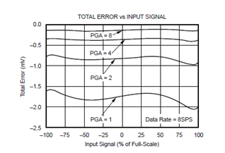
    However, the "total error vs input signal" graph conveys an error as high as -1.5 .. -2.0 mV for PGA=1.

    What is that in LSB?

    If I remember correctly: LSB = V_FSR / 2^N
    For a Vcc= V_FSR = 5 V and N=15 bit resolution (single ended use), 1 LSB ~ 0,15 mV.
    Thus the total error is about 10 .. 13 LSBs ( ~ 3.5 bit).

    If that is correct, doesn't this "total error" reduce the "effective resolution", say by at least 3 bit to 12 bit?

    Please bear with me if that is too crude a calculation for you.

    Thanks.

    Best regards,
    Daniel

  • Hi Daniel,

    This topic originated with noise and now you have moved on to total error which would include all error sources such as offset, gain, noise, INL, etc..  Effective resolution is limited to noise only or the ability of the ADC to resolve to a specific level.  If we look strictly at the noise component, we can see that with data rate increased the resolution will decrease as is shown in Table 1 on page 6 of the ADS1100 datasheet.

    As to the total error, the error sources are converted to the same units and then an RSS analysis is used to calculate the total error.  Some of these sources can be calibrated or adjusted to limit the effects of the error.  Gain error can often dominate and becomes more pronounced as the input approaches full-scale while the offset error may be more flat.  In the end the total error will appear to be bow-tie like over the input range where the worst case appears at full-scale and narrows as the input approaches 0.

    So total error effects overall accuracy while effective resolution determines the capability of the ADC to resolve to a specific level of precision.  Let's say we have 2.5mV of offset, which will effect the overall accuracy of the measurement.  But let's say we remove the 2.5mV of offset by calculation in post processing which then improves the accuracy of the measurement.  The actual precision of the measurement remains unchanged as in one case the result includes the offset while the second case the offset is removed.

    If you think of a target and you shoot arrows at a bullseye (or target center) you see that the arrows may be closely grouped together but is off to the right and above the center.  This would be precision shooting (every shot is closely repeatable), but not accurate due to the offset of the arrow grouping.  If the offset is removed, then the arrows become both accurate and precise.  I hope that makes it a little more clear.

    Best regards,

    Bob B