This thread has been locked.

If you have a related question, please click the "Ask a related question" button in the top right corner. The newly created question will be automatically linked to this question.

ADS52J90: TI204 IP rx data output

Part Number: ADS52J90
Other Parts Discussed in Thread: , LMK04826

Hi,

I'm trying to run the ADS52J90 with the JESD interface and the TI204 IP. I realized know ,that the TI204 IP generates I and Q related output values, so it sees always a pair of adc channels are related to each other. But I need just seperated normal adc values, how could I achive that?

Best,

Manuel

  • Hi Manuel,

    Thanks for reaching out. 

    Due to multiple requests I was not able to look at this one. Please allow me to go through the TI JESD IP and shall let you know how you know what can be done.

    As far as I know I think it gives individual channel data only. What do you mean by pair of adc channels related to each other? I could not follow this part of your question. can you please explain. Also, please share if any images are there.

    thanks & regards,

    Abhishek

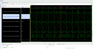
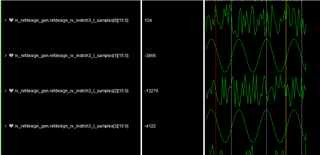
  • The problem is when I connecting only ch9 of the ADS52J90EVM Board of the ADC to a 2MHz sinus signal I'm measuring the proper sinus signal in the Xilinx ILA (see picture)

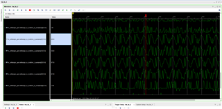
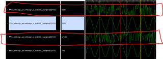
    But If I connect another 2MHz signal to the CH11 of the EVM I get the following results 

    As you could see I don't have anymore a proper sinus but still some high signals on four channels. It seems to be somehow correlated, that was why I thought it could be some kind of IQ conversion either integrated in the IP or the ADC.

    Now the question is does this problem comes from your IP or maybe also from the ADC? Or could it be something else?

  • Hi Manuel,

    Can you share some more information about your setup. Below are a couple of questions:

    1. What is the speed? Are you using 16 channel mode?

    2. NUM_ADC_PER_LANE =? (it is equivalent to serialization of 40x, 80x, and 160x)

    3. Are you using the demod? If so, what is the settings such as decimation factor, compression factor etc?

    4. Can you try data capture with internal test patterns from the device and see if the obseved data makes sense.

    5. What are the different data lines in your ILA corresponds to such as ch4_I_samples[0]?

    To my view, I think the problem might be related to configuration of the device.

    Thanks & regards,

    Abhishek 

  • Hi Abhishek
    below you could find my answers numbered to your questions.

    1. Further inforamtions
        ADC parameter:
        Speed = 1.562 Gbps
        FPGA GTX clock = 156.25 MHz
        FPGA/ADC SysREF = 4.8828125MHz
        ADC Clock = 39.0625 MHz
        FPGA clock = 156.25MHz
        Mode = 16 Channel Mode

        Jesd Parameter:
        L = 8
        M = 16
        S = 1
        F = 4

    2. Number ADC per lane = 2

    3. demodulation:
        The Demod node I don't wana use, but I don't know which register belongs to it. Therefore it is possible that it is switched on but I don't want to use it!
        Could you send me the demod registers because in the data sheet these registers are missing.

    4. Test pattern
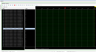
        I used the ramp test pattern, this looks ok for all channels:


    5. Configuration:
        cml_1 = ADC1 and ADC2
        cml_2 = ADC3 and ADC4
        cml_3 = ADC5 and ADC6
        cml_4 = ADC7 and ADC8
        cml_5 = ADC9 and ADC10
        cml_6 = ADC11 and ADC12
        cml_7 = ADC13 and ADC14
        cml_8 = ADC15 and ADC16

        Measured in with ILA:
        ADC1 = CH3_I_samples[0] and CH3_I_samples[2]
        ADC1 = CH3_I_samples[0] and CH3_I_samples[2]
        ADC1 = CH3_I_samples[0] and CH3_I_samples[2]
        ADC1 = CH3_I_samples[0] and CH3_I_samples[2]
        ADC1 = CH3_I_samples[0] and CH3_I_samples[2]
        ADC1 = CH3_I_samples[0] and CH3_I_samples[2]
        ADC1 = CH3_I_samples[0] and CH3_I_samples[2]

    Finally here are the ADS52J92 EVB configuration file:

    ADS52J90_16ch_SINE_8L_16x_14b_GBLCLKDIV1_FSDIV4_SYSREFDIV32_20x_TI204_ip.cfg

  • Hi Manuel,

    Thanks for sharing the desired information. 

    Let me have a look and understand the problem and get back to you.

    Thanks & regards,

    Abhishek

  • Hi Abhishek,

    How is your status. Could you estimate when I get an answer? 

    Because if I don't solve that problem soon I had to look for another ADC.

    Many Thanks

    Manuel

  • Hi,

    I still have troubles with ADC values on the same lane as you could see before. Still waiting for an answer there?

    Today I was measuring the sync-serdes output and there was always a low signal. therefore I want to ask you how could I set the TI204 IP to Subclass 1? 

  • Hi Manuel,

    Sorry I was unavailable due to emergency.

    I looked at the data you have shared. I have some doubts about the data you have shared:

    1. 1. Further inforamtions
        ADC parameter:
        Speed = 1.562 Gbps = 39.0625 x 16 bits x 2 Channels x 10 bit/8bit  = fs x 40 (40x serialization) ; the device is doing 40X serialization

        FPGA GTX clock = 156.25 MHz (Why are you setting this frequecy?) Is the deserialization in FPGA happening at 10x speed?
        FPGA/ADC SysREF = 4.8828125MHz - please check if this is indeed the right frequency.
        ADC Clock = 39.0625 MHz
       FPGA clock = 156.25MHz - please check this
       Mode = 16 Channel Mode

    I think you should first check your clocking scheme. From the config file you shared, I think you are using LMK04826 in clock divider mode and your divide factors are 1 for fpga_gtx clock, 4 for adc_clk, and 1 for fpga_clk. However, in the original config file, i think its different. i.e 1 for fpga_gtx clock, 2 for adc_clk, and 4 for fpga_clk

    Next,

    3. Demod: To disable the demod, please write Reg3[0] - EN_DEMOD =  0; I can share you the demod register map. Please send me a separate email, regarding the same on abhishek.vishwa27@ti.com

    4. Ramp: The ramp pattern does not seem proper, it is always an upward slope ramp and when it hits the full value its reset and start again. Also, I think it is not 14 bit ramp pattern since its repeating quite fast.

    By the way, are you using the customer EVM & TSW14J56 capture solution or building your own capture solution with another FPGA?

    If you are using the customer EVM, can you share the clocking connections, Also, if possible can you look at the clock outputs using an oscilloscope and check whether they are correct.

    Thanks & regards,

    Abhishek

  • Hi Manuel,

    The JESD settings seems okay. Just ensure ENABLE_JESD_VER_CONTROL bit in register 115 is set to 1. Also, ensure that you are appropriately writing the JESD_WR_SEL in Reg3 while writing to JESD registers.

    Thanks & regards,

    Abhishek

  • Hy Abhishek,

    Many Thanks for your answers.

    1. For the parameters I tried to stay as close as the example design from you. Is 40x serialisation a problem for the chip or do I have to take something into account for that?

    The FPGA GTX clock is 156.25MHz because I'm using the same as FPGA clock. Is there something I need to know about choosing the GTX clock? How do you end up with deserialization of 10x on the FPGA?

    I will go over my clocking scheme, I'm just not sure what frequency to use for the GTX clock and how it is related to the others.

    3. I will send you a mail for the demod register specs.

    4. Thanks for the hint. Now that I know the output is wrong I could start to verify with the test pattern again

    5. No I'm not using the TSW14J56 cause it is obsolete. I'm using the ZCU102 from Xilinx. I verified the clock outputs with the Oscilloscope maybe it is worth to do it again.

    Thanks and regards Manuel

  • HI Abhishek,

    I'm tryning to use the JESD204B subclass 1, so why I have to put then the ENABLE_JESD_VER_CONTROL to 1? Does the TI204 IP not support the subclass 1?

  • Hi Manuel,

    Yes, you are right, by default the device will be in subclass 1, JESD204B. I just mentioned that it in case you want to change, ensure to set the ENABLE_JESD_VER_CONTROL. That's all.

    Thanks for confirming that you are not using TSW. However, you have the customer EVM of the ADS52J90 right?

    Can you tell which input clock is going to LMK04826 device? Is it 40 MHz oscillator, or coming from the external connector? Since the config file is configuring the LMK in clock divider mode, I am assuming, you must be giving external clock on the SMA connector. Am I right?

    Regarding the FPGA Gtx clock:

    As I explained, since the device is sending the data at lane rate of 1.562 Gbps, in order to do that the device is effectively doing the serialization at 40x. So, it is generating the clock which is Fs x 40. Hence in your case it is :39.0625 x 40 MHz = 1.562 GHz.

    Similarly at the FPGA end, the fpga is receiving the serial data at 1.562 Gbps and it has to do deserialization, typically I have seen that the FPGA uses fixed 40x deserialization (can you confirm this). Hence the GTX clock to the FPGA should be same as ADC CLK (only if deserialization inside FPGA is 40x). 

    Otherwise, you have to scale the GTX clock accordingly to match the lane rate at the device end and FPGA end.

    For example, say in 4 lane mode:

    Fs x 4 Channel x 16 bit x 10b/8b = Fs x 80 --> 80x serialization

    Say, FPGA deserialization factor is 40x.

    Then to match the lane you have:

    Fs x 80 = Fgtx x 40

    Hence Fgtx (FPGA_GTX CLK) will be = 2 x Fs

    I hope it helps.

    Thanks & regards,

    Abhishek

  • Hy Abhishek,

    Yes, for the ADS52J90 I'm using your EVM ADS52J90EVM.

    I realised that I used the wrong SYSREF clock, cause it has not been a multiple of the LMFC clock. Therefore I changed the SYSREF divider from 32 to 40. In the attachment you could find the new config File.

    6685.ADS52J90_16ch_SINE_8L_16x_14b_GBLCLKDIV1_FSDIV4_SYSREFDIV32_20x_TI204_ip.cfg

    Unfortunately also with the new SYSREF I got the old problems.

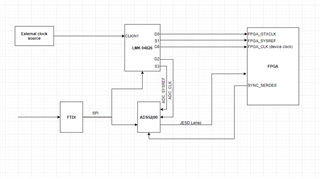
    The clock connection is done like the following picture, with an external input clock source of 156.25MHz:

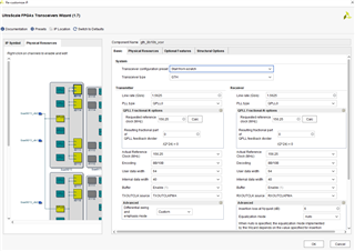
    For the FPGA GTX clock I couldn't found any options for deserialization. I just have the possibility to set the reference clock and the lane rate as you could see next:

  • Hi Manuel,

    The clocking scheme seems fine.

    Regarding the configuration of the JESD transceiver IP, let me check with someone in my team about the correct configuration.

    Will get back to you by tomorrow.

    Thanks & regards,

    Abhishek

  • Hy Abihishek,

    I was looking on the results I get from your IP. And I thinking probably the mapping of the data is wrong. so could you send me probably something in more detailed about it as your data sheet on page 56 Table 24. 

    Regards,

    Manuel

  • Hy Abihishek,

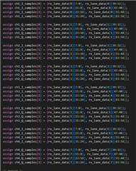
    I enabled the scrambling and adjusted the mapping of the data as shown afterwards:

    Now the channels are running as expectedt!

    Could you explain what for signal will be generated on the unused channels (ch3_i_sample[0][15:0] and ch3_i_sample[3][15:0])? Are this artefacts from the a demodulation?

  • Hi Manuel,

    I suppose the demodulator is off. Hence there can be no artifacts. 

    What do you mean by unused channel? You have all the channels data coming on all the CML lanes right? If no input is given to the ADC channel then, you should see simply noise. However from the data i can see the amplitude is high? could this be due to 2s complement.

    Also, you can try internal test patterns such as constant pattern, ramp etc on individual channels to correlate the correct mapping.

    Thanks & regards,

    Abhishek

  • Hy Abhishek,

    One lane is coming on 64 Bit output stream of your IP as follows:

    Now on the channel ch3_i_samples[1] and ch3_i_samples[3] i got the sine wave signals from the ADC. On the other two arrays ch3_i_samples[0] and ch3_i_samples[2] I get noisy data:

    So these channels I meant with unused channels. 

    Regards,

    Manuel

  • Hi Manuel,

    I think you should reconfigure the IP to 2 ADC per channel. Hence the data width should be 32 bits not 64 bits. 

    Currently looking at your data, i looks like the FPGA is expecting the data from 4 adc channels.

    Thanks & regards,
    Abhishek

  • Hi Abhishek,
    Then where could I specify the IP to have only 2 ADC per lane?

    Beside that i noticed that I only reach half of the sample rate i should reach with my clocking scheme. Maybe this is also related to that issue with the 2 ADC per channels.

    Thanks & regards,

    Manuel

  • Hi Manuel,

    I have shared your case with internal TI JESD IP expert. 

    He will guide me to properly configure the IP. Once I hear back from him, I'll let you know what is the expected changes you need to make.

    Thanks & regards,
    Abhishek

  • Hi Manuel,

    Below is the feedback I have received.

    "

    The computation of the line rate of 1.5625Gbps seems accurate. The reference clock to the transceiver can be any frequency from the drop-down link (as the PLL in the transceiver will scale it back to the line rate).

    If you choose the deserialization width of 64, each clock cycle (on the rx_sys_clock side) will be 19.53125MHz, and the IP will generate 2 samples / cycle for each ADC. If the deserialization is reduced to 32 bits, you will need to modify some of the parameters of the JESD IP to get it to work (I believe I had originally generated it for 64 bit width).

    "

    Can you change the deserialization width to 32 bits and check if the data is coming properly. 

    Thanks & regards,

    Abhishek

  • Hi Abhishek, 

    I already tried to reduce the width from 64 bit down to 32 bit, unfortunately without  success. Then I reduced the Lanes from 8 to 4, because at the end I have to go anyway to 4 Lane operation. For 4 Lanes operation I guess 64 Bit width should be ok right?

    But until know also the 4 Lane operation doesn't work.