This thread has been locked.

If you have a related question, please click the "Ask a related question" button in the top right corner. The newly created question will be automatically linked to this question.

DAC63204EVM: DAC63204EVM

Part Number: DAC63204EVM
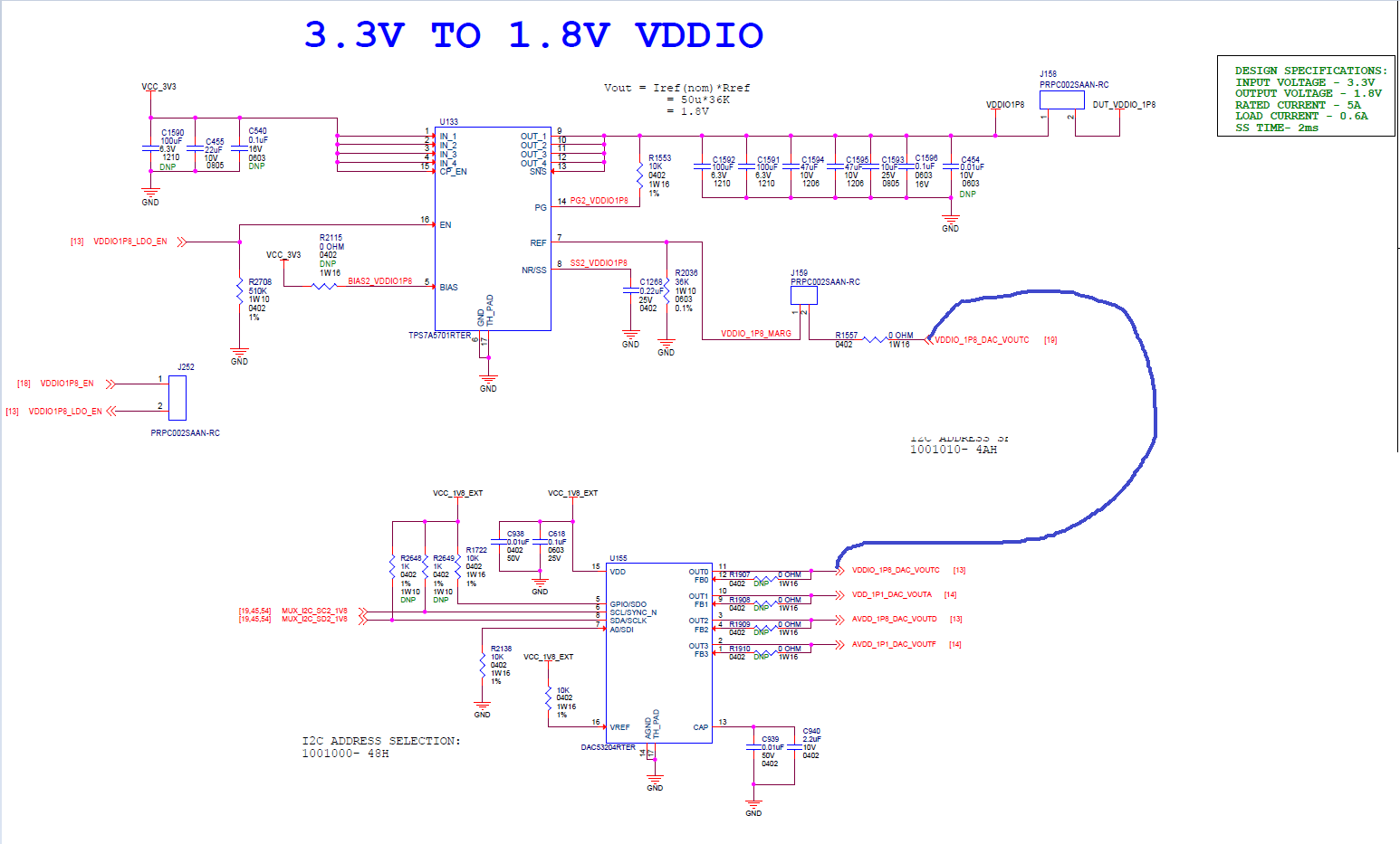
Other Parts Discussed in Thread: TPS7A57

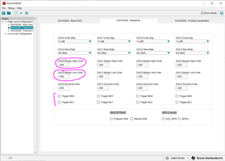
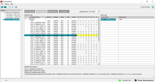
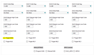
If i drive NVM setting it showing error like. (THIS ERROR is returned by the shared library function).

and also if i change nominal to high or low code its not changing it showing 000. 

  • Hi Sri,

    I had also run into an issue using the NVM checkbox recently so I need to investigate this error and update the GUI. For now, can you try going to the low level page and writing 0x0002 to register 0x20? This will also program the NVM.

    For your second issue, what exactly is showing 000? Are you saying that the input fields do not update after you write a new value and press enter? Can you try reading the device ID and making sure you get the correct value? I want to make sure that you actually have successful communication with the EVM. 

    Best,

    Katlynne Jones

  • Hi Katlynne Jones,

    Thanks for the response.

    We have used this DAC family part in our design and we are trying to this check DAC performance with EVAL board.

    I would need a Favour from TI side.

    We are used in Current and voltage mode. Could you please help us to share the configuration file? It will be help full.

    Based on this we will implement for other VR's.

    Below is our circuit connection for current mode -

    Below is our circuit connection for Voltage mode -

  • Hi Dhanabal,

    Were you able to read the device ID successfully? 

    I would need more information on what you are actually trying to configure with the device. 

    For voltage mode I am going to assume you are using the internal reference with 1.5x gain and no slew rate enabled. Margin high of 0xFFF and margin low of 0x000. It doesn't look like you are using the GPI pin to trigger any output, so use the software triggers in the COMMON_DAC_TRIGGER register. 

    The setup would be:

    Registers|DAC_0_MARGIN_HIGH FFF0
    Registers|DAC_0_MARGIN_LOW 0000
    Registers|DAC_0_VOUT_CMP_CONFIG 0800
    Registers|DAC_1_MARGIN_HIGH FFF0
    Registers|DAC_1_MARGIN_LOW 0000
    Registers|DAC_1_VOUT_CMP_CONFIG 0800
    Registers|COMMON_CONFIG 1FC9
    Registers|COMMON_DAC_TRIGGER 0000

    VOUT.cfg

    For current mode I am assuming you are using the smallest range with no slew. Nominal code 0x80 (0A), margin high 0xFF (25uA), margin low 0x00 (-25uA). 

    The setup would be:

    Registers|DAC_0_MARGIN_HIGH FF00
    Registers|DAC_0_MARGIN_LOW 0000
    Registers|DAC_0_IOUT_MISC_CONFIG 1000
    Registers|DAC_1_MARGIN_HIGH FF00
    Registers|DAC_1_MARGIN_LOW 0000
    Registers|DAC_1_IOUT_MISC_CONFIG 1000
    Registers|DAC_0_DATA 8000
    Registers|DAC_1_DATA 8000
    Registers|COMMON_CONFIG 0FF6
    Registers|COMMON_DAC_TRIGGER 0000

    IOUT.cfg

    Best,

    Katlynne Jones

  • Hi Katlynne jones,

    Even if i try to Load code it  not Load. Once again it Comes with default settings. Even after entering code in low Level config it shows same error as(This error is returned by shared library function).And Not able to get Reference Voltage. It gives as 5V.

    Regards,

    R SRI RAJA SUMAN

  • Hi Sri,

    So any change to the low level page results in the error? There may be an issue with your GUI installation. Can you do a complete uninstall and reinstall the GUI?

    Best,

    Katlynne Jones 

  • Hi katlynne jones,

    Registers|DAC_0_MARGIN_HIGH FFF0
    Registers|DAC_0_MARGIN_LOW 0000
    Registers|DAC_0_VOUT_CMP_CONFIG 0800
    Registers|DAC_1_MARGIN_HIGH FFF0
    Registers|DAC_1_MARGIN_LOW 0000
    Registers|DAC_1_VOUT_CMP_CONFIG 0800
    Registers|COMMON_CONFIG 1FC9
    Registers|COMMON_DAC_TRIGGER 0000

    My jumper settings is removed J6 and using I2C

    What is the expected Output voltage for this code? And also how to load NVM for this Code in Low level configuration.?

    Regards,

    R SRI RAJA SUMAN

  • Hi Sri, 

    You can click file -> open config and select the .cfg files that I attached. The GUI will load the configuration. Or, manually write each value by clicking on the value column for each register and entering the value. To save the NVM, write 0x0002 to register 0x20 in the low level configuration page. The expected output is 0V for nominal, 2.1816V for margin high, and 0V for margin low. You would need to configure these values to be specific for your margining requirements. 

    Best,

    Katlynne Jones

  • Hi katlynne,

    How did you calculate Vout 2.1816v for Margin High(FFF0)?

    I'm getting 1.816 For you High margin code.

    My calculation:  Vout= DAC_DATA/ 2 N × VREF × GAIN

    Vout=(4095)/2^12*1.21*1.5

    Vout=1.816 I'm getting in Dac Vout.

    Is this way i'm calculated Vout is right?

    And also need Iout calculation

    Regards,

    R SRI RAJA SUMAN

  • Hi Sri, 

    You are correct, I think I just had a typo in the number or messed up in my equation. VOUT is 1.816V

    The IOUT margin high value value for the sequence I shared is IOUT = [(DAC_DATA * IMAX − IMIN)/ 2^8 ]+ IMIN = [(255*25uA+25uA)/2^8]-25uA = 24.8uA.

    Best,

    Katlynne Jones 

  • Hi katlynne ,

    I have 3 doubts.

    1) I got Iout 25ma but if i change bits its not changing current it stays as 25ua. Range values from -25 to 25 not getting.

    2) 1000: -25 µA to +25 µA
        1001: -50 µA to +50 µA
        1010: -125 µA to +125 µA
        1011: -250 µA to +250 µA

    If i want 55ua what should i do is there any way what to get 55ua by changing bits? Can i get Iout value required for me?

    3) For a current mode o/p should i remove FB resistors? is this necessary to remove it for Iout.

  • Hi katlynne,

    Today I've tested in Iout mode with the below config

    DAC_1_MARGIN_HIGH as E600

    DAC_1_MARGIN_LOW 0000
    DAC_1_IOUT_MISC_CONFIG 1000

    DAC_1_DATA 8000
    COMMON_CONFIG 0FF6
    COMMON_DAC_TRIGGER 0000

    E600 for 20uA and R6 resistor on the Eval board. Measured using 6 1/2 multimeter at the Dac Out_1 on the Eval board But it measures 26uA instead of 20uA. Please check the config which i written in the Low level config table . The same issue observed for 50uA,125uA,250uA.

    Regards,

    R SRI RAJA SUMAN

  • Hi Sri, 

    You are not required to remove the FB resistors, but you can to minimize leakage through the FB pins:

    To get 55 μA you should set the device in the ‒125 μA to +125 μA range: set DAC-X-IOUT-MISC-CONFIG (0x04) to 0x1400 and set DAC-X-DATA (0x19) to 0xB800.If you want to use the margin high register, then set the register to 0xB800 and use the margin high trigger to change the output. Directly writing to the margin high register will not change the output, you have to also use the trigger.

    You can do that on the high level page, or also by writing 0x2000 to the COMMON-DAC-TRIG (register 0x21)

    It also looks like you are setting the range for channel 0, but setting the margin high for channel 1. So make sure you are writing everything to the right channel and using the right trigger bit. 

    Best,

    Katlynne Jones 

  • Hi Katlynne Jones,

    Thanks for the clarification.

    We are trying to do the voltage margining for the TPS7A57 LDO.

    This LDO ref pin is 50uA as the reference current. So 50*36K=1.8V will get as a Typical voltage.

    We will need to margin +/-10% voltage of 1.8V, it will be 1.62V and 1.98V.

    So If we are forcing +/- 5uA from the DAC, we will be getting 1.62V and 1.98V in the output. Is my understanding is correct?

    Based on the understanding, today in our lab we loaded below config file and tested the O/P.

    When we measure the o/p using 6 1/2 DMM - Its always stays at 25uA.

    Registers|DAC_0_MARGIN_HIGH E600   ------------For 5uA margining
    Registers|DAC_0_MARGIN_LOW 0000
    Registers|DAC_0_IOUT_MISC_CONFIG 1000
    Registers|DAC_1_MARGIN_HIGH E600   -------------For 5uA margining
    Registers|DAC_1_MARGIN_LOW 0000
    Registers|DAC_1_IOUT_MISC_CONFIG 1000
    Registers|DAC_0_DATA 8000
    Registers|DAC_1_DATA 8000
    Registers|COMMON_CONFIG 0FF6
    Registers|COMMON_DAC_TRIGGER 000

    Trigger we will be using SW trigger.

    Could please confirm whether we are following the right procedure?

    Please help to generate the config file for the above scenario(Margin the LDO with +/- 10%? It will be help full.

    Regards,

    Dhanabal.K

  • Corrected the config file address -

    Registers|DAC_0_MARGIN_HIGH 9A00------------For 5uA margining
    Registers|DAC_0_MARGIN_LOW 0000
    Registers|DAC_0_IOUT_MISC_CONFIG 1000
    Registers|DAC_1_MARGIN_HIGH 9A00-------------For 5uA margining
    Registers|DAC_1_MARGIN_LOW 0000
    Registers|DAC_1_IOUT_MISC_CONFIG 1000
    Registers|DAC_0_DATA 8000
    Registers|DAC_1_DATA 8000
    Registers|COMMON_CONFIG 0FF6
    Registers|COMMON_DAC_TRIGGER 000

  • Hi Dhanabal,

    Your understanding of the margining current is correct. 0x9A00 is correct for +5uA from the DAC. Margin low should be 0x6600 for -5uA from the DAC. The config file looks correct. 

    Can you read back all of the registers in the low level page to make sure they were actually written to? The only thing I can think of that is setting the output to 25uA is that margin low is set to 0 code. This would actually be -25uA, but that depends on the polarity your probes are connected. You would only be seeing the -25uA if you are sending the margin low trigger command. If not, the output should not be defaulting to 25uA so I am not sure why you would be seeing that. 

    One possible issue here is going to be the compliance voltage of the current mode outputs. The voltage at the output of the DAC channel needs to be 400mV below VDD or 400mV above GND in order for the DAC to regulate the output current:

    Your supply voltage is 1.8V which is not 400mV above your intended voltages on the VREF pin of the TPS7A57. Try increasing the VDD for the DAC. 

    Best,

    Katlynne Jones