A related question is a question created from another question. When the related question is created, it will be automatically linked to the original question.
If you have a related question, please click the "Ask a related question" button in the top right corner. The newly created question will be automatically linked to this question.
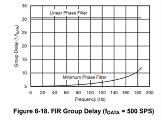
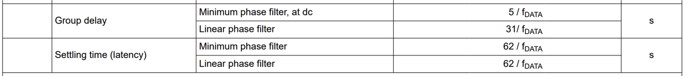
ADS1285: Do you have the group delay data for 1285
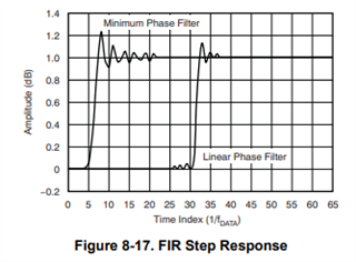
could you share the delay curve calcualtion formula showed in FIR group delay picture?
Is this what they are looking for? Let me know if they need help calculating f_DATA.
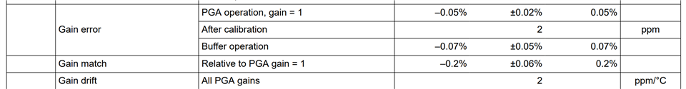
Note, that group delay and gain error are completely independent. Gain error is considered a DC error that deals with the difference of input compared to the output for no gain vs. high gain. Group delay refers to when a sample appears at the output compared to the input. Essentially, this is delay vs. error, they are not comparable unless the user is looking at non-settled data and wondering why there is error in non-settled data. Non-settle data is not a valid data point to compare performance.
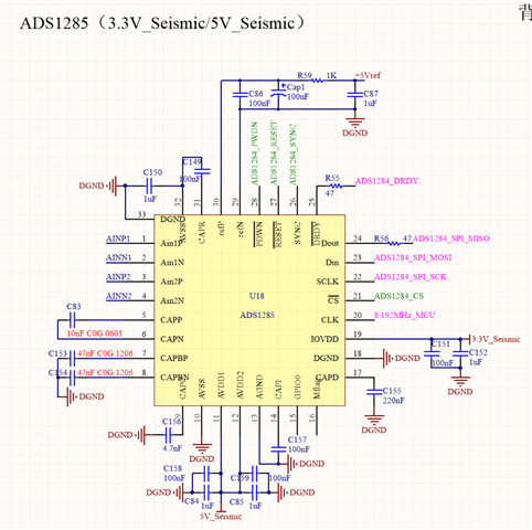
now customer (AIWEIBISI) test their board, and find their gain error reach 11%.
This result is out of specification when compared to the datasheet. So, its not the device's fault. We expect <+/-0.05% and 11% means there is something completely incorrect coming into the PGA of the ADS1285.
I suggest they compare the voltage on the input pins (AINPx and AINNx) and the input voltage signal (ain+???). In other words, can they bypass their analog front end and apply the test voltage to the pins directly? Or at least describe their input set up for testing.
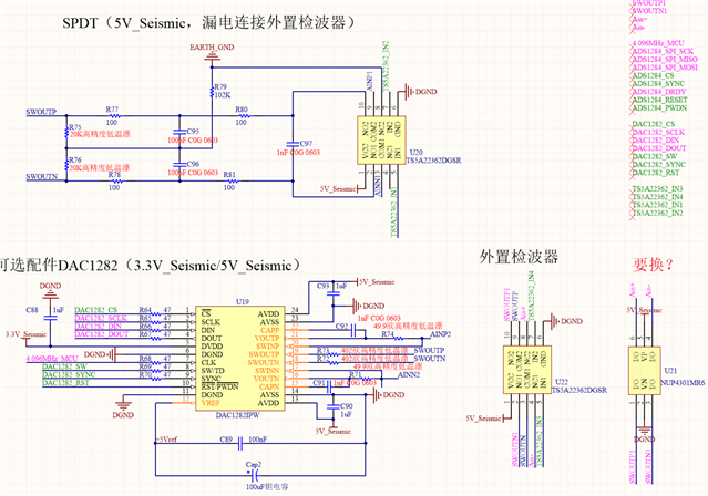
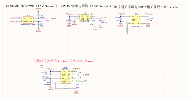
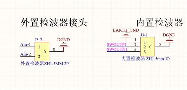
I think a lot of the required components for the ADS1285 look good. However, I do not understand their MUX input voltage circuit. I don't know what kind of performance TS5A22362 offers. This is why I would like them to bypass MUX and go directly to the input. The reference circuit looks good from what I can tell.
I noticing having >50 ohms on the input (R78, R77, R81, etc) drastically affected THD. I am curious if this might be contributing.
I have not had a change to look at it thoroughly. I still need to look at the reference path and SWOUTx path. I will say, all of the decoupling capactiors (CAPx) look very far away. I will have to check them out in more detail later.
My other questions:
Are they testing with the DAC1282? It looks like there's a direct path from DAC1282 DACOUT to AINx2. Have they compared their current results to this DAC1282 path?
Also, tomorrow is a US holiday. Please expect some delay in the response.
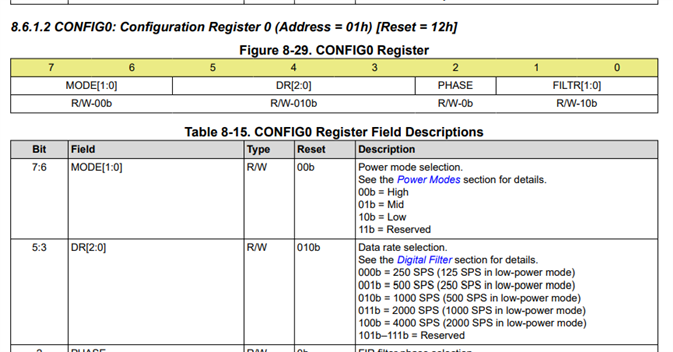
They are using 8.192MHz nominal as told in their schematic so that would be mid or high power mode. That means it is the number of the left (250SPS - 4000SPS).