This thread has been locked.

If you have a related question, please click the "Ask a related question" button in the top right corner. The newly created question will be automatically linked to this question.

AMC60704: IDAC Output Performance

Part Number: AMC60704


Hello,

I'd like to ask some questions about AMC60704's IDAC output performance.

Questions

  • The data sheet defines 0.4 V as the Min output compliance voltage of the AMC60704's IDAC, but what can happen if the IDAC output voltage goes below 0.4 V?
    • I wonder if some parameters can go out of the specs but the device operates normally. Or, can the device show unexpected behavior? If the IDAC output voltage below 0.4 V is not allowed, the AMC60704 cannot be used for my design.
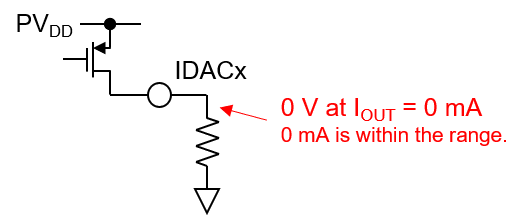
  • In the application, a small amount of IDAC output current within the IDAC zero-scale error specs is suspected to flow out of the output from the observation of the load circuit's behavior when the current setting is 0 mA, but there is no means to confirm it. I'm wondering if an equivalent block diagram of the IDAC buffer amplifier is available because it could help identify the cause of the issue. Could you provide me with the IDAC buffer amplifier's equivalent circuit?

Best regards,
Shinichi Yokota

  • Hi Yokota-san,


    The device won't be damaged but the output will not behave as expected. I don't have a plot for this use case, but the device will not be able to regulate the current output if the minimum compliance voltage, similar to plot 6-38 in the datasheet when the minimum headroom requirement from PVDD is not met. 

    I can't share the equivalent output architecture or a block diagram beyond what is shown in the datasheet. Similar to any DAC, the output of the DAC resistor ladder has inherent zero code and full scale errors and any buffered DAC has an offset error due to the offset of the amplifier. If the IDAC is set to zero code then the measured output current is a combination of the offset and zero code errors. You can measure this once with a resistive load if you're concerned that your load is adding additional error. 

    Best,

    Katlynne Jones 

  • Katlynne,

    The device won't be damaged but the output will not behave as expected. I don't have a plot for this use case, but the device will not be able to regulate the current output if the minimum compliance voltage, similar to plot 6-38 in the datasheet when the minimum headroom requirement from PVDD is not met.

    Is the Min value "0.4 V," in fact, a headroom from the PVDD? Is the correct description of the specs "PVDD - 0.4 V" (Min) and "PVDD - 0.2 V" (Max)?

    I thought the MIn value "0.4 V" is from GND and wondered why.

    Best regards,
    Shinichi Yokota

  • Hi Yokota-san,

    The min is 0.4V from ground. You could call it "footroom" instead of headroom. Violating the 0.4V compliance voltage will have a similar behavior to violating the headroom requirement to PVDD. 

    Best,

    Katlynne Jones 

  • Katlynne,

    I'm afraid I don't get the point yet.

    I guess that the AMC60704's IDAC buffer amplifier only sources an output current and it doesn't sink. From that, I suspect that the IDAC buffer amplifier's output stage needs only pMOSFET hung from the PVDD or the equivalent circuit. If that's correct, the IDAC output compliance voltage can be 0 V. On the other hand, the IDAC's output current range is from 0 mA and if the load is resistive to GND, for example, the IDAC output voltage becomes 0 V when the output current is 0 mA. The Min spec "0.4 V from GND" of the IDAC output compliance voltage implies that such an usage is not allowed for the AMC60704.

    I suspect that a pull-down function in power-down mode has something to do with the "0.4 V from GND" spec, but can the spec be relaxed depending on the IDAC output current? For example, "0 V from GND" is OK at the output current of 0 mA, that I'd like to ask.

    Best regards,
    Shinichi Yokota

  • Katlynne will respond after the US holiday weekend.

  • Hi Yokota-san,

    Sorry for the delay, I am trying to ask the designer to see if they can help with an explanation. Please give another day or two. 

    Best,

    Katlynne Jones 

  • Hi Yokota-san,

    I got some feedback from the designer as to why the minimum compliance voltage spec exists.

    1. The circuits you shared are good equivalent circuits.

    2. Purely from a circuit perspective, there is no reason the compliance needs to be >0.4V, which agrees with your analysis. The IDAC can drive into 0V. However, the issue is power dissipation and long term reliability of the pfet. If the customer is driving 200mA into 0V with PVDD=2V, Pdis=400mW/ch, and self heating will likely become an issue. But if the die temp can be kept below 125C, this is not an issue. If PVDD>2V and the device is outputting high current for any extended period of time, there is an issue with reliability from hot electron effect on the pfet.

    The output is fine driving into 0V as long as PVDD<2V and die temp<125C.

    Best,

    Katlynne Jones 

  • Katlynne,

    Thanks for your support. Could you consider adding a note of that description in the data sheet? Otherwise, I suspect that some customers would be confused with the Min spec 0.4 V of the IDAC output compliance voltage.

    Best regards,
    Shinichi Yokota

  • Hi Yokota-san,

    You're welcome. I can discuss adding a note with the systems team. They likely chose the minimum to avoid any chance of the reliability concern, but I see how it can be misleading. 

    Best,

    Katlynne Jones