This thread has been locked.

If you have a related question, please click the "Ask a related question" button in the top right corner. The newly created question will be automatically linked to this question.

ADS1278EVM-PDK: Daisy chained ADS1278 not staying in sync

Part Number: ADS1278EVM-PDK
Other Parts Discussed in Thread: ADS1278

Hello,

I am using two ADS1278 that are both part of the EVM-PDK kit, but using the MMB0 only for power. I have them configured in SPI daisy chain. They are both configured for high resolution mode and TDM/fixed output.

I am not able to make sense of the data that I am getting with the two parts in daisy chain. I was able to successfully read 8 channels from one part. Now I am trying to read 8 channels from one part and 4 from the other. I am looking at the signals to and from each chip to make sure things are working because I am not getting good data even from the U2 chip (using the naming from the datasheet figure 81) which I would assume would act basically as if it is not daisy chained for the first 8 channels worth of clocks.

What I am doing: I have slowed CLK to 512kHz to see if there are problems with my connections at high speed and that didn't seem to improve things but I am leaving it that way while I figure this out. I have not been power cycling the ADCs while testing this (maybe I have to do that?). When my MCU boots it

1. sets the SYNC pin high

2. enables the 512kHz clock

3. waits for 2^18/512kHz + 129/1kHz (0.641 seconds). This is my attempt to wait until data appears (as recommended by the datasheet) without reading the DRDY pin directly. This timing comes from Figure 84. Start-Up Sequence. and the note to wait until data ready before asserting SYNC is in the sentence immediately above that figure in the Feb 2011 revision of the data sheet.

4. after data ready (really just a delay as described above) I bring the SYNC pin low for 10 us and then high again (CLK not stopped during this).

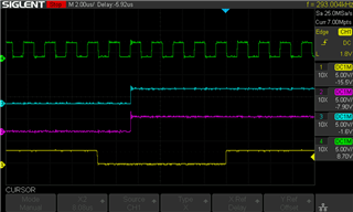
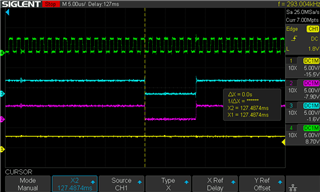
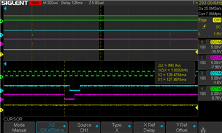
When I watch this on the scope I see that after bringing SYNC low and then high the DRDY pins from both chips stay high for about 129 Tdata periods as the datasheet says will happen. Then the first DRDY low edge from both chips is indeed aligned to the same clock falling edge as expected. However the next data ready pulse from the two chips is not aligned. I just did this and the DRDY falling edge from one chip (U2 as per the datasheet naming) was 3 clocks later than the DRDY falling edge from U1. As I let this run the DRDY edges do not remain in sync and shift in time with respect to each other.

The datasheet says I need to examine the DRDY pin from only U1, but I am wondering if I should expect that DRDY from both chips should remain in sync.

Perhaps there is something wrong with the way I am doing the sync operation?

  • So one issue I discovered is I wasn't waiting long enough (with the lower speed I am using for debugging) between the DRDY falling edge and starting the SPI clock. Adding a delay of one CLK period in the beginning of my DRDY interrupt before starting SCLK seems to have fixed the data coming from U1. Now that the data from channels 1-8 (U1) is mostly good I can clearly see that the effect of DRDY on U2 being out of sync in that sometimes the data makes sense, and periodically it is complete garbage (because I am reading in the middle of conversions on U2). So this leads me to believe the the answer to my question (if I should expect that DRDY from both chips should remain in sync) is yes I should expect that, and now I am just wondering why that is not the case.

  • Here are some scope shots for reference.

    Here green is CLK, magenta is DRDY from U1, cyan is DRDY from U2, and yellow is SYNC (probed at the MCU).

    This is the sync pulse. I think this makes sense.

    This is the first DRDY pulse. This also makes sense. It is at (roughly) the right time, and the falling edges are aligned to one CLK edge as expected.

    This is the second DRDY after the SYNC pulse. This is where the DRDY edges start to diverge (here U2 is delayed by one CLK period).

  • Here is an example of what the two DRDY signals look like when they are far out of sync.

    Green is U2 DRDY, cyan is U1 DOUT, magenta is U1 DRDY (this triggers the SPI transactions), and yellow is SCLK.

    U2 DRDY has become so far out of sync that new samples are occurring at times while a transaction is ongoing.

  • Interestingly I was just measuring the duration between two pairs of DRDY falling edges. I have been saying that the U2 DRDY starts coming late after initially being in sync with U1 DRDY. What I just found, however, is that on the first DRDY cycle after SYNC when U1 and U2 DRDY do not match it is U1 DRDY that is one clock early. I am not sure what would make that so. I am not actually counting CLK edges (because apparently my scope can't do that) but I am just measuring the time between DRDY edges, and it looks like U1 is the one that is incorrect, not U2.

  • Hello Colin,

    Using the same clock source for both ADS1278's and sending the SYNC pulse should result in both DRDY signals staying synchronized.  Since this appears to work correctly immediately after the SYNC pulse, I think this part of the timing is working.  However, since the DRDY pins are getting back out of sync, this suggests that the CLK's are different for each ADC.

    My guess is that the CLK is either the wrong logic levels or has a lot of ringing, causing the ADC's to interpret a different number of clock edges.  Since you are running at a low clock frequency of 512kHz for debug purposes (SCLK must be less than or equal to 512kHz in this case) you may want to try cleaning the clock edges up a bit by adding a small RC filter on each ADC clock pin.

    Try getting a good measurement directly at the clock pin of each ADC using your scope to see if there is any substantial ringing.

    It looks like you have everything setup correctly, so I think you should be very close to getting this to work.

    Regards,
    Keith Nicholas
    Precision ADC Applications

  • Green is CLK at the output from my MCU, magenta and cyan are CLK at TP8 on the EVM board.

    Not sure if that is significant ringing or not. Also interesting that the slew rate setting of the MCU CLK output is seemingly defeated by the EVM CLK mux U6. I wonder if it would be worth connecting the CLK lines directly to TP8 to bypass U6 rather than to J4.17 as I have now.

  • What I did here is remove the jumper on SW6.3, connect the jumper on SW6.5 to SW6.4, and moved my CLK wire from J4.17 to J4.5. This allows me to bypass U6 without having to make some poor connection to TP8. Now all the CLK signals match up much better (green/magenta/cyan all overlaid), and there seems to be less ringing overall.

  • Using this configuration seems to have improved things. The DRDY edges are no longer shifting fully out of phase with each other, but they are not staying aligned either.

    This is a recording of the two DRDY signals as I start my processor. They start aligned, but quickly shift to 9 or 10 CLK cycles from each other and they seem to remain there indefinitely.

  • Hello Colin,

    Hopefully this is good enough to evaluate your system and develop some code.  I do think this is a signal integrity issue, and now that the clocks are more cleaned up, it is working better.

    When you develop a custom PCB with both ADS1278's and a common clock, SYNC, and other SPI, I do not think you will see this issue again.  This is the first time I have seen this behavior.

    Regards,
    Keith

  • Thanks Keith!

    That is the conclusion I have come to as well. This makes me feel comfortable enough to move forward with a custom board.