This thread has been locked.

If you have a related question, please click the "Ask a related question" button in the top right corner. The newly created question will be automatically linked to this question.

ADS1278: Design Review

Part Number: ADS1278


Hello E2E Experts,

Good day.

I review those tutorials on the TI website, but I think the filter design front of the anti-aliasing filter is not declared to me.
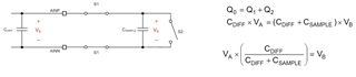
It is because I have mentioned that the accelerometer's analog output range is between +/- 4 V, and the ADS1278 is +/- 2.5 V.
Does the charge bucket's capacitor could reduced input analog voltage by changing C_DIFF?
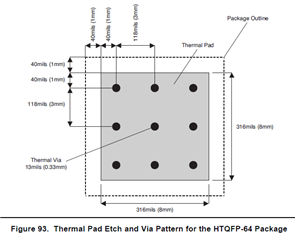
Besides that, I just try to place thermal via on my PCB design, but it seems that design rule check have lots of error.
I place the copper area around the thermal pad, and place the via inside this area, am I right? or I make any mistake?
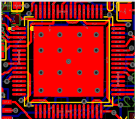
My project: https://easyeda.com/editor#id=|bab4aa8fc55e413e817f7be4dfbb5163|630e61dee0b34477a06e66baf5cee80f|49afe0f440334dafa7f7fe6afb4c0247I
I look forward to hearing from you, thank you.
Regards,
CSC
  • Hello,

    Thank you for your post.

    The antialiasing filter is not intended to scale the analog input voltage. Any signal conditioning (i.e. gain, filtering, etc.) is typically achieved in a separate section of the input signal chain. You can consider using a fully-differential amplifier like the THS45xx family to drive the input signal to the ADC while also scaling amplitude to +/- 2.5 V.

    These FDA devices can also be used to set the input common-mode voltage of the ADC input pins. The ADS1278 expects a typical common-mode of mid-supply (i.e. 2.5 V). There is an internal common-mode pin (VCOM) which can be externally buffered and connected to the FDA VOCM pin. See Figure 87-88 for example.

    You may need to adjust your layout design rules according to the recommended layout information in the data sheet. Figure 93 shows the recommended thermal patch etch and via land pattern for the ADS1278 HTQFP-64 package. There is also additional land pattern information at the end of the data sheet. 

    Regards,

    Ryan

  • Hello Ryan,

    Good day.

    My understanding of your following suggestion, the charge bucket is not providing any signal attenuation.
    Does it mean there is no signal that has been scaled down in my circuit?
    If I do not change any part of my recent circuit, could my circuit pull with an SDI accelerometer that has +/- 4V differential input?
    About thermal via, I knew that I should follow the datasheet to put on my PCB,
    but I think it is a little bit complicated for me to do it on EasyEDA (even though it is named "Easy" EDA).
    Would you have any recommendations? or do I need to change other tools to finish it?
    Besides, I already spent a lot of time on this PCB design, but there are still so many parts of research that I need to finish, including algorithms and some programming.
    I apologize for my weak knowledge and poor questions, but I really need to move on with my research.
    Regards,
    CSC