This thread has been locked.

If you have a related question, please click the "Ask a related question" button in the top right corner. The newly created question will be automatically linked to this question.

ADS1220: Problems ads load cell balance

Part Number: ADS1220

hello people,
I have a problem with the ads 1220 and a load cell.

I have an assembled board with 2 individual ads that handles 2 load cells a left and a right load cell.

the ads are managed by SPI connection with an adafruit

The problem I am having is that for no apparent reason when I turn on the equipment one of the load cells stops taking the measurement.

to take the measurement again I have to turn off and turn on the equipment again.

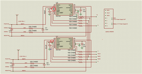
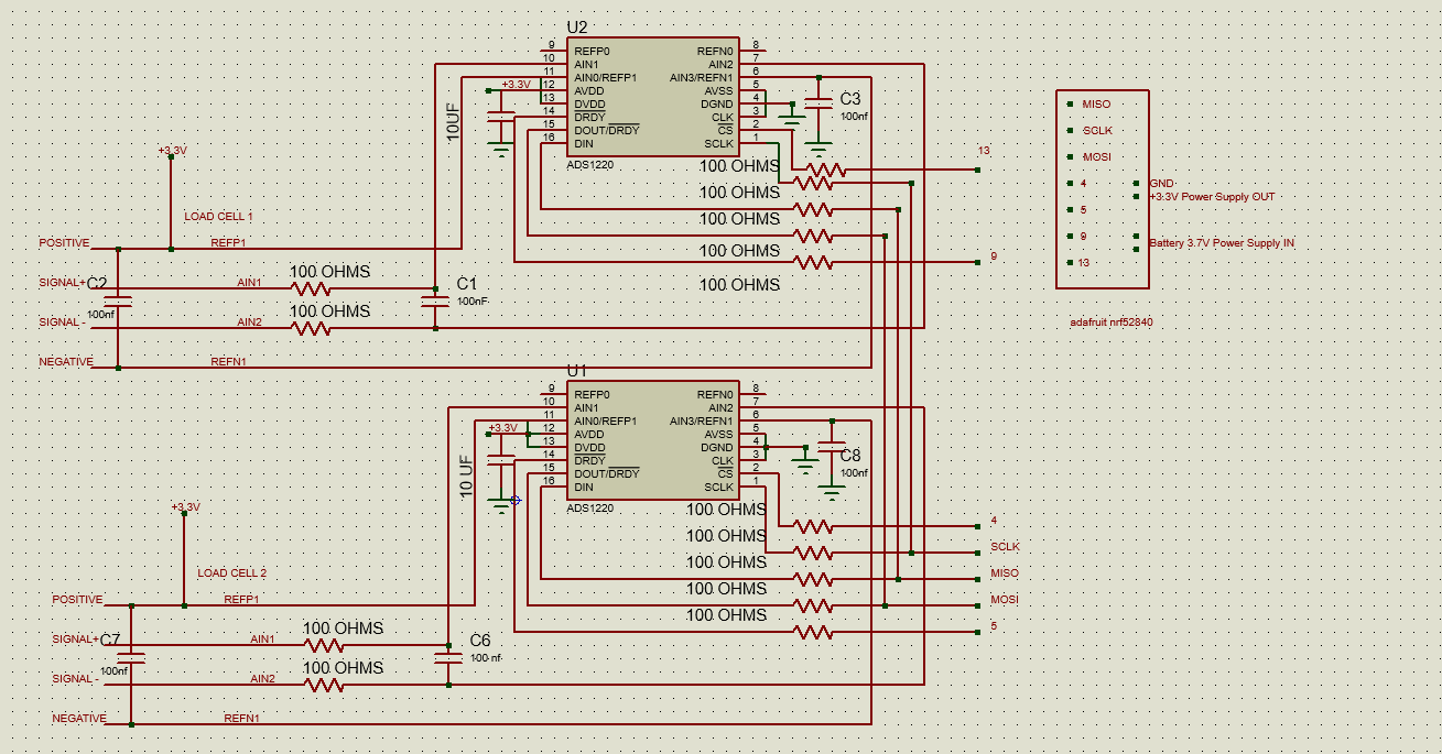
I am attaching the diagram of the PCB with the ads and the load cell data.

Thank you very much for your help.
Load Cell 

Specifications:

Range:  100, 150, 200, 250, 300, 350, 500 (KG)

Accuracy : C2

Temp. effect on span(%F.S/10℃): ±0.02

Comprehensive error(%F.S) : ±0.02

Temp. effect on zero(%F.S/10℃) : ±0.03

Rated output(mv/v) : 2.0±0.1

Compensated temp. range(℃ ) : -10~+40

Creep(%F.S/30min) : ±0.02

Use temp. range(℃ ) : -20~+60

Zero balance(%F.S) : ±1.0

Excitation voltage(V) : 9~12(DC)

Input resistance(Ω) : 405±10

Safe overload (%F.S) : 120

Output resistance(Ω) : 350±3

Ultimate overload (%F.S) : 150

Insulation resistance(MΩ) : ≥5000(100VDC)

Defend grade : IP65

  • Hi ,

    Can you please clarify the following questions?

    1. When you turned on the equipment, was the ADC not work immediately or it stopped working after worked for a while? 
    2. When you said "stops taking the measurement", did you mean no available /DRDY signal from the ADC or you always got constant data (no change)?
    3. Did the phenomenon always happen on a particular device (U1 or U2)?

    Thanks.

    Regards,

    Dale

  • Hi ,

    There is one more question, did you write the internal registers to close the switch between AIN3/REFN1 and AVSS and also select the right input channel (AIN1 and AIN2) which is not default input channel?

    Also, can you please clarify your the following connections in your schematic below which are highlighted in red?

    Thanks&Regards,

    Dale

  • Hello again. Thank you for your prompt reply.

    I will answer the questions you asked me in order.


    1. When you turned on the equipment, was the ADC not work immediately or it stopped working after worked for a while? 

     R: It is relative, sometimes you turn on the equipment and only one load cell works and sometimes both work and after a while 1 cell stops working.

    2 -When you said "stops taking the measurement", did you mean no available /DRDY signal from the ADC or you always got constant data (no change)?

    R: I am not so sure about this at this point I should connect a logic analyzer and wait for the failure to happen and see what happens in the DRDY....
    When I say that it stops receiving data I mean that in the serial monitor of the arduino IDE the cell does not take measurement while the other cell continues to take the measurement. 

    3  Did the phenomenon always happen on a particular device (U1 or U2)?

    R:

    To repeat a little of what was said in the previous answer, what happens is that

    you turn on the equipment and only 1 cell works indirectly, either U1 or U2.

    it can happen that you turn on the equipment and none of the two cells work.

    it can happen that both cells work without any problem and without reason 1 or both cells stop working.

    to take measurement again it is necessary to restart the equipment.

    but even if sometimes you restart it does not mean that they will work, many times it is necessary to restart it several times.

  • There is one more question, did you write the internal registers to close the switch between AIN3/REFN1 and AVSS and also select the right input channel (AIN1 and AIN2) which is not default input channel?

    R: I wouldn't be sure if I did that or not.
    If you're telling me programmatically, I'm not sure I have the right code to do that.
    It may be that it is in the ADS library that is loaded in the programming.
    Would you have an example to reference. 

    Also, can you please clarify your the following connections in your schematic below which are highlighted in red?

    the connections that you ask me about in red is a bridged connection, i.e. those three ADS tracks are linked together. 

  • other data to be taken into account.
    the frequency rate that I take the data from the adafruit to the ADS is at a frequency of 1Khz.

    The ADS as shown in the diagram are fed at a voltage of 3.3 volts from the output of the adafruit's internal regulator.

    I don't know if this is important since the load cell says that the output voltage is 9 to 12 V DC and it is being fed with 3.3V.

    another question.
    Could it be that the internal REFN1 switch is being discounted, that's why the ADS shuts down and stops taking a reading.

    Could AIN 1 be used with REFP0 and REFN0 ?

    The lack of capacitors as shown in the example diagram in the datasheet may affect its operation.

  • There is one more question, did you write the internal registers to close the switch between AIN3/REFN1 and AVSS and also select the right input channel (AIN1 and AIN2) which is not default input channel?

    I don't know if this code is adequate 

    void ADS1220::setPowerSwitch(uint8_t value) {
    /* Configures behavior of low-side switch between AIN3/REFN1 and AVSS.
    0 - Always open
    1 - Automatically closes when START/SYNC command is sent and opens when
    POWERDOWN command is issues.
    */
    // Make sure the value is in the valid range. Otherwise set to 0x00
    if (value > 0x01) {
    value = 0x00;
    }
    value = value << 3; // Shift to match with mask
    writeRegisterMasked(value, REG_MASK_PWR_SWITCH, CONFIG_REG2_ADDRESS);
    }

  • Hi Federico,

    To make them clear, let me separate my questions with your answer and your further questions as below:

    ------------------------------------------------

    DL: 2 -When you said "stops taking the measurement", did you mean no available /DRDY signal from the ADC or you always got constant data (no change)?

    R: I am not so sure about this at this point I should connect a logic analyzer and wait for the failure to happen and see what happens in the DRDY....
    When I say that it stops receiving data I mean that in the serial monitor of the arduino IDE the cell does not take measurement while the other cell continues to take the measurement. 

    DL:  It's hard to just check serial monitor of your Arduino for debug. I would suggest to use a logic analyzer or an oscilloscope to check your timing from only one ADC as the first step.

    -------------------------------------------------

    DL: 3  Did the phenomenon always happen on a particular device (U1 or U2)?

    R:  To repeat a little of what was said in the previous answer, what happens is that

    you turn on the equipment and only 1 cell works indirectly, either U1 or U2.

    it can happen that you turn on the equipment and none of the two cells work.

    it can happen that both cells work without any problem and without reason 1 or both cells stop working.

    to take measurement again it is necessary to restart the equipment.

    but even if sometimes you restart it does not mean that they will work, many times it is necessary to restart it several times.

    DL:  What's your power supply for the ADCs? Please make sure your power supply circuit can provide enough power to these devices. 

    -------------------------------------------------

    DL: There is one more question, did you write the internal registers to close the switch between AIN3/REFN1 and AVSS and also select the right input channel (AIN1 and AIN2) which is not default input channel?

    R: I wouldn't be sure if I did that or not.
    If you're telling me programmatically, I'm not sure I have the right code to do that.
    It may be that it is in the ADS library that is loaded in the programming.
    Would you have an example to reference. 

    DL: I would suggest you to develop your own code instead of using a library which may not be verified and fully tested, you will have a better understanding to know what the issues are caused. Without programming the internal registers and configuring the ADCs properly, you are not able to get any data from the ADC. For example, your input channel pair (AIN1 and AIN2) is not default input channel, so you have to select them in the internal Configuration register 0.

         You can see the example code at the bottom of the page in the link:  ADS1x20 Example Code

    -------------------------------------------------

    DL: Also, can you please clarify your the following connections in your schematic below which are highlighted in red?

    R: the connections that you ask me about in red is a bridged connection, i.e. those three ADS tracks are linked together

    DL: It seems that no dot on these connections in your schematic, you can check if they are connected well on your real circuit board. 

    ---------------------------------------------------
    R: the frequency rate that I take the data from the adafruit to the ADS is at a frequency of 1Khz.

    The ADS as shown in the diagram are fed at a voltage of 3.3 volts from the output of the adafruit's internal regulator.

    I don't know if this is important since the load cell says that the output voltage is 9 to 12 V DC and it is being fed with 3.3V.

    another question.
    Could it be that the internal REFN1 switch is being discounted, that's why the ADS shuts down and stops taking a reading.

    Could AIN 1 be used with REFP0 and REFN0 ?

    The lack of capacitors as shown in the example diagram in the datasheet may affect its operation.

    DL: I'm not sure whether your are using the default 20sps data rate or not. If you are configuring the device at a higher data rate, you need a fast SCLK frequency to retrieve the data.

          I would suggest you to either externally apply a known DC signal or configure internal register to select an internal test signal ((AVDD+AVSS)/2 or (AVDD-AVSS)/4 ) instead of using load cell for test purpose, and then you can check if your code match your DC input signal.

         Answers to your questions: 

         a. the low-side power switch is designed and used for a bridge application. It will not affect ADC's operation and data conversion as long as you have proper configurations (input channel and reference selection).

         b. the input configuration on this ADC is flexible,  so yes, it can be used with an external reference on REFP0 and REFN0, and also you can use internal reference for test purpose to make sure your ADC operation and your timing are correct. Note that an input pair should be selected and configured in the Configuration Register 0, both AIN1 and AIN2 should be selected in your case.

    ----------------------------------------------------

    DL: There is one more question, did you write the internal registers to close the switch between AIN3/REFN1 and AVSS and also select the right input channel (AIN1 and AIN2) which is not default input channel?

    R: I don't know if this code is adequate...

    DL: I do not know how the function of writeRegisterMasked() works. Again, I would suggest you to develop your own code instead of using a library which may not be verified and fully tested.

    ---------------------------------------------------

    Regards,

    Dale