This thread has been locked.

If you have a related question, please click the "Ask a related question" button in the top right corner. The newly created question will be automatically linked to this question.

ADC78H90: ADC78H90

Part Number: ADC78H90

Hi Ti Expert,

We are using ADC78H90 ADC to one of our important product line.

The interfacing of ADC78H90 to STM32H723VGT6 MCU over SPI communication is not working properly. 

 This is a showstopper for our R&D. Could you please kindly do the needful to support us to resolve the same?

Kindly let me know what information you need it.

We can have a online call also if needed.

Thanks.

Snehashis

  • Hi Snehashis,

    Can we start looking at your ADC78H90 with a screen cap that shows the /CS, DIN, DOUT and SCLK lines between the chip and processor?

  • Hello Tom,

    Just to clarify from my side, you want to to check the DSO output captured for those signals or Circuit diagram?

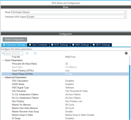
    Meanwhile, I can provide you certain data from SPI master configuration for MCU.

    And below is the command I am sending to read the AIN1, AIN6,AIN7 and AIN8.

    const uint8_t aTxBuffer[] =

    {0,14,40,0,
    0,14,48,0,
    0,14,56,0,
    0,14,0,0};

    This data was sending with AT32UC3C1512C MCU to read the same information from ADC.

    Right now we can able to see some data which are not expected.

    If possible could you please check this configuration and the command once and suggest the needful?

    Thanks.

    Snehashis

  • It's much easier to look at an oscilloscope or logic analyzer screen capture than it is to sort through your code since I don't specifically know that processor.

  • Hello Tom,

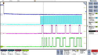
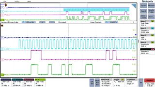
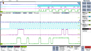
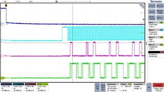
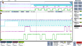
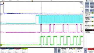
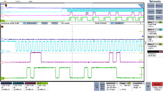
    We have captured those 4 pins for all the combination of clock polarity and clock phase mode. For every mode we took two screenshots.

    1. All 4 signals

    2. Zoomed version of SCLK, MOSI, MISO signals for the better view.

    Please find the below:

    Combination 1: Clock Polarity = LOW, Clock Phase = 1st Edge

    ===============================================

    Combination 2: Clock Polarity = LOW, Clock Phase = 2nd Edge

    ===============================================

    Combination 3: Clock Polarity = High, Clock Phase = 1st Edge

    ===============================================

    Combination 3: Clock Polarity = High, Clock Phase = 2nd Edge

    ===============================================

    Could you please check and please suggest us what we need to do?

    Thanks.

    Snehashis

  • Hi Snehashis,

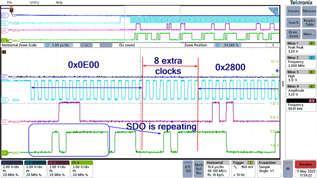
    First thing is that you should probably consider using the SPI in its native 'burst clock' mode, with /CS toggling for each 16 bits sent to the ADC78H90 - it is easier to manage the communications in my humble opinion.  If you look at the second combination 3 above (CPOL=1, CPHA=1), you are transmitting 0x0E000028000...  There are 'extra' clocks being transmitted and the ADC is shifting out the conversion result a second time before your next channel command is being decoded.

    So - you never really did say what is wrong with the SPI communication, but I suspect you are not expecting to see the SDO repeat and that you are capturing data incorrectly.

  • Hello Tom,

    I cannot say that I understood the problem and the solution properly.

    My requirement is simple , to read the AIN channels from the ADC over SPI.

    If possible could you please refer any Example Firmware which I can refer to interface this ADC over SPI, or, if possible can we have a online call?

    Thanks.

    Snehashis

  • In a nutshell - you are sending 24 clocks to the ADC between CHx commands when you should only be sending 16.  Get rid of the extra clocks or toggle the /CS pin high between your channel commands.

  • Hello Tom,

    Thank You . I will take care that.

    Before that , if possible could you please confirm me certain configurations parameter?

    CPOL & CPHA Configuration 

    Combination 3: Clock Polarity = High, Clock Phase = 2nd Edge(Sampling at even clock)

     Command buffer  to read the AIN1, AIN6,AIN7 and AIN8.

    const uint8_t aTxBuffer[] =

    {0,14,40,0,
    0,14,48,0,
    0,14,56,0,
    0,14,0,0};----------------------> I believe here lies the issue

    Moreover, we have kept clock frequency as 20 MHz

    And SCLK, MISO, MOSI lines put high sped but no pull up or pull down.

    If possible could you please suggest?

    Thanks.

    Best Regards,

    Snehashis

  • Snehashis,

    20MHz SCLK is fine.  CPOL=1, CPHA=1 is fine.  You do not need pull ups/downs on the control lines.  I prefer to think in terms of HEX values, so to read CH0, CH6, CH7, CH8 you would write 0x0000, 0x2800, 0x3000, 0x3800.  Refer to Tables 1-3 on page13.  The '14' you have above is E in hex, which gives the 0x0E00 I pointed out earlier.  That would actually select CH2.  Since the channel command spans 2 nibbles - bits 7, 6, 2, 1 and 0 are 'don't care'.  You set bits 3, 2 and 1 with that command.

  • Hello Tom,

    Thank You very much for confirming.

    Let me check the same. Because of time difference(IST), I will execute the same on tomorrow and will let you know the result.

    Thanks Again.

    Best Regards,

    Snehashis

  • Hello Tom,

    In our system we have 3 such ADC ICs which are selected by CS pins.

    One of the ADC IC is connected with the voltage 1.853 Volt(Tested and confirmed with multimeter) at AIN1. We sent 16 bit data 0x0000 and receiver buffer is also 16 bit. On sending the command 0x0000, we are receiving 0x5fe, which implies the sensed voltage as 1.236 volt.

    When we tried to read the AIN2 with 0x2800 command, we read the same data 0x5fe.

    We captured one of such data exchange in the below screenshot.

    We can see 32 clocks.

    Now, we are confused why  ADC sends 0x5fe for 1.853 Volt and whether it expected that again 0x5fe data is repeating for both 0x0000 and 0x2800 commands.

    Moreover, even though I selected other 2 ICs using CS pin, all those data from AIN1 and AIN2 are coming as 0 only.

    If possible could you please check and suggest if any mistake is happening from MCU side?

    Thanks.

    Snehashis

  • Your MOSI is not what you expect it to be.  You are in CPOL=1, CPHA=0 mode in that screen capture above.  Change the phase and see if it makes a difference.  By default, the ADC78H90 selects CH1 at powerup.  You also need to keep in mind that the channel you select in cycle 'N' will provide conversion results in cycle N+1.   What is your AVdd supply voltage?  The 0x5FE sounds about right for a 1.853V input when using a 5V supply.

  • Hello Tom,

    Yes, regarding the Clock Phase , I will change it and try.

    Regarding the AVdd supply voltage, it is 3.3V.

    Thanks.

    Best Regards,

    Snehashis

  • Hi Tom,

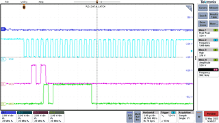
    I have configured the Master Clock Polarity = High, Clock Phase = 2nd Edge  i.e. CPOL=1,CPHA = 1 and still did not receive the proper data for ~ 1.86 volt where AVdd as 3.3 v.

    Please find below the screen captured from logic analyzer.

    Could you please check once and let me know if I need to change anything?

    Thanks.

    Best Regards,

    Snehashis

  • Hi Snehashis,

    The ideal output would be something like 0x8F8 and you are at 0x8EB, so you are not that far off.  I'd need to review your schematic to see where improvements can be made in the conversion results.

  • Hi Tom,

    That is not 0x8EB. That is 0xBEB.

    Probably the picture does not have that much of zooming. 

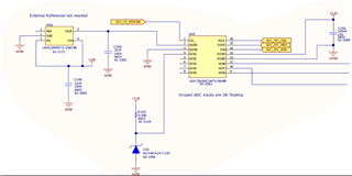
    Below is the screenshot of the schematic.

  • Hi Tom,

    Moreover, I was checking another same IC for AIN2. SPI master sent command 0x0800 but it always reads 0 which is also not correct.

    Thanks.

    Snehashis

  • That looks like a 2.7V zener on AIN1.  0xBEB would be ~2.45V.  Can you probe AIN1 with an oscilloscope while you are doing conversions?  I'd like to see if there is any bounce during the conversion process.

  • Hello Tom,

    The issue is resolved. PS for the AVdd supply voltage was not stable immediately after we turned on. So, the ADC was sending correct value based on AVdd supply voltage at that instant.

    Thank You very much for your kind support.

    We are closing this thread.