This thread has been locked.

If you have a related question, please click the "Ask a related question" button in the top right corner. The newly created question will be automatically linked to this question.

DAC7811: DAC7811 Gain is not updating as expected

Part Number: DAC7811

Hi team,

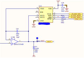
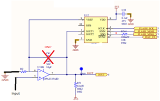
            We are using  DAC7811 in our project(through SPI communication) to control the gain of ADC signals. While working we noticed that the GAIN which we are trying to set is not applying currently. I have some doubts regarding this ,

1. Is there any sample code available for DAC7811 to control the gain through program ? , if yes please provide the reference here.

2. what is the default gain of this DAC7811( in datasheet it is mentioned like "The device powers on with zero-scale loaded into the DAC register and IOUT lines", does that mean the gain is zero?

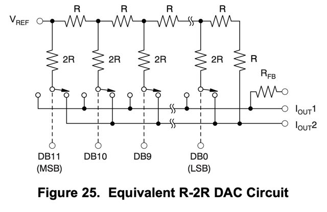
3. the first 4 bits, i.e. C0- C3 is the main as per datasheet , there is a option for readback the DAC register or its value, if I write 0x2XXX where does it will provide me the readback value?

4. if I am not using daisy chain mode , is it mandatory to disable that while reading nd writing into DAC? , does this has any effect even though I am not using it.

regards,

Shikamaru

  • Hi Shikamaru-san,

    Sanjay will review and help here.

    Thanks,

    Paul

  • Could you share your schematic as well?

  • I want to know from the software side as well. for all the above queries which are mainly focusing on the programming part of DAC.

    here is the schematic for your reference.

  • Hi Shikamaru,

    Hope you are having a great day !

    Please check the response for your queries - 

    1. We do not have any code examples for this device.

    2. As you can see in image that by default IOUT1would be high impedance node, there wouldn't be any gain.


    3. You should send additional 2 bytes for read-back on SDO pin

    4. No, it will not have any affect even though you are not using it

    Note : I looked at your design and i am not able to make any sense how it's going to work. Please look carefully on this and feel free to get back, would be happy to help further.

    Thanks,

    Sanjay

  • Thanks Sanjay for your response,

    3. You should send additional 2 bytes for read-back on SDO pin

    For this I need clarity, DAC shift register is of 16 bit, out of which 4 bits is used for controlling it's operation and remaining are the Data bits. So in this case along with this 16bit (2 bytes) need to send 2 more bytes is it ? which will result into 32 bit buffer(4 bytes total).

    Note : I looked at your design and i am not able to make any sense how it's going to work. Please look carefully on this and feel free to get back, would be happy to help further.

    Can you share your inputs on this. it will be helpful for our consideration.

  • Hi Shikamaru,


    3. You should send additional 2 bytes for read-back on SDO pin >> it means that write normal DB[15:0] (16 bit data frame) with control bits value b'0010 and this will give the last written data on SDO.


    and regarding your design, can you provide details of what is intended application of this ? 

    Thanks,

    Sanjay

  •   

    Here is the complete schematic. we are planning to use it as a feedback resistor instead of DAC to dynamically change the gain of this non inverting amplifier. The value of R2 is 487 ohm. 

  • Hi Shikamaru,

    Now this seems to be okay. 

    Thanks,

    Sanjay

  • Thanks Sanjay

  • Hi,

    We are using the above circuit to achieve the variable gain amplifier. When we set the gain to 64, with input voltage of 28mV we are getting the output voltage of 1.6V. However, when the input voltage increases to 36mV with gain of 64 the output of the amplifier is saturating. 

    We would like to know why the amplifier output is saturating.

    Thanks,

    Sreekanth

  • Hi Sreekanth,


    When you say gain of 64, can you please explain how you getting it. I Meantime, i will check about saturation part of it.


    Thanks,

    Sanjay

  • Hi Sanjay,

    In the schematics attached by Shikamaru, know input signal is applied and the gain is set via SPI. With calculation (As we know how many R is enabled)  we know the gain. 

    So when the input voltage increases the gain is also increasing. From firmware we are not changing the gain. Gain is fixed for testing. Please do let us know why the gain is getting increased with input voltage.

    Thanks,

    Sreekanth 

  • Hi Sreekanth,


    It's highly unlikely that gain will change with Vin. Can you please provide the some more detail : 

    1. Vin vs Vout (at the IOUT node) table/plot

    2. VDD node voltage, R2/R71 values.


    Thanks,

    Sanjay