Hi,
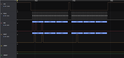
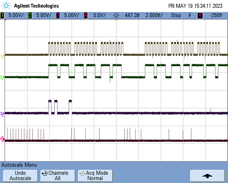
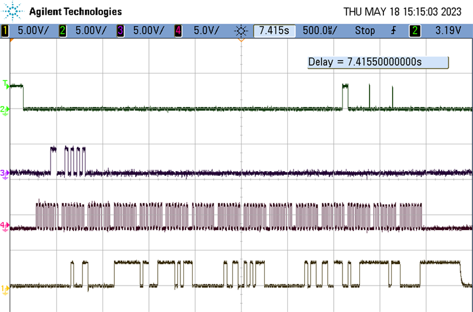
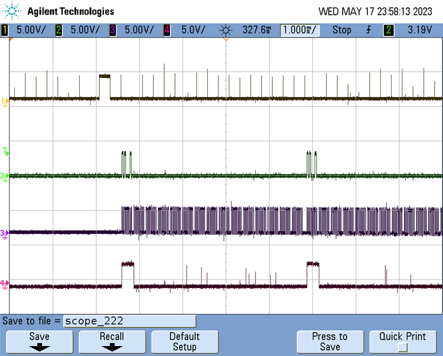
I am using the ADS131M03 with the raspberry pi 3B and program through python. The ADC is clocked by an 8.192 MHz external MEMS oscillator. The SPI rate is set at 32 kSPS (I also tried 3.2 k and 320 Hz). The system previously worked in the protoboard but not working in the PCB. The captured waveform is shown as attached (First: DRDY, Second: Datain, Third: SCLK, 4th: Data out). I was trying to read the Gain register, but it returns 255 response and none of the channel data (same results while trying to read 0x00 register), which is clearly not correct.
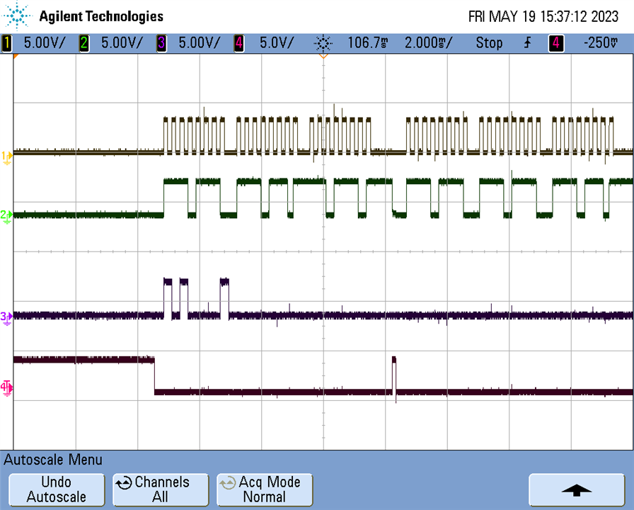
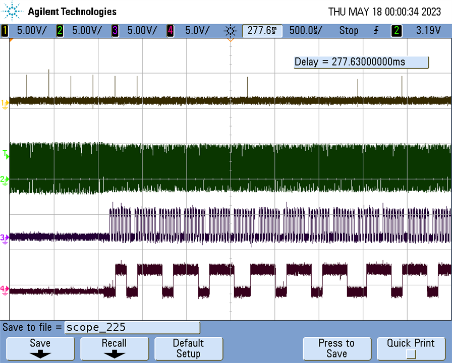
One interesting thing is that when I was trying to probe to CLKIN pin (which is connected to the external clock), the chip is able to output readout results but different each time, the captured waveform is attached: (1st: DRDY, 2nd: CLKIN, 3rd: SCLK 4th:Dataout)
The codes I am using is attached, I used the 0.0000125 delay in reset pin to sync but seems not working.
import time
import spidev
import RPi.GPIO as GPIO
import sys
# clk is a mini class to generate a Master-Clock signal over a PWM Pin


#and also a function which gets two hex numbers and gives back the "Message" for send
#settings
GPIO.setmode(GPIO.BCM)
GPIO.setup(17, GPIO.IN, pull_up_down=GPIO.PUD_UP)   #Pin 17 --> DRDY Pin
GPIO.add_event_detect(17,GPIO.FALLING)

GPIO.setup(8, GPIO.OUT)                             #Pin 8 --> CS'
GPIO.output(8,1)
GPIO.setup(2, GPIO.OUT)                             #Pin 2 --> RESET/SYNC
GPIO.output(2,1)
spi = spidev.SpiDev()

spi.open(0,0)
spi.mode=0b01                                       #CPOL=0, CPHA=1; resting state = 0, data read at falling edge

spi.max_speed_hz =32000
spi.bits_per_word = 8
spi.lsbfirst = False


def read():
    GPIO.output(8,0)
##    time.sleep(0.000125)
##    GPIO.output(2,0)
##    time.sleep(0.000125)
##    GPIO.output(2,1)
##    time.sleep(0.000125)
    send_data = [0b10100000,0b10000000,0b00000000,0b00000000,0b00000000,0b00000000,0b00000000,0b00000000,0b00000000,0b00000000,0b00000000,0b00000000,0b00000000,0b00000000,0b00000000]
    com_reg=spi.xfer2(send_data)


    if GPIO.event_detected(17):
        send_data = [0b10100000,0b10000000,0b00000000,0b00000000,0b00000000,0b00000000,0b00000000,0b00000000,0b00000000,0b00000000,0b00000000,0b00000000,0b00000000,0b00000000,0b00000000]

    # read null response
        com_reg=spi.xfer2(send_data)
##        com_reg=spi.readbytes(15)
        result1 = (8388608-abs(com_reg[3]*256*256+com_reg[4]*256+com_reg[5]-8388608))*0.00000014
        result2 = (8388608-abs(com_reg[6]*256*256+com_reg[7]*256+com_reg[8]-8388608))*0.00000014
        result3 = (8388608-abs(com_reg[9]*256*256+com_reg[10]*256+com_reg[11]-8388608))*0.00000014
        result1 = str(result1)
        result2 = str(result2)
        result3 = str(result3)
        time1 = time.strftime("%H:%M:%S ")
        print("channel1: "+result1+" V")
        print("channel2: "+result2+" V")
        print("channel3: "+result3+" V")
        print("read2")
        print (com_reg)
        file.write("prototest  ")

        file.write(time1)
        file.write("channel1: "+result1+" V  ")

        file.write("channel2: "+result2+" V  ")

        file.write("channel3: "+result3+" V")
        file.write("\n")


    GPIO.output(8, 1)
    time.sleep(1)

def Gain_config():
    GPIO.output(8,0)
    if GPIO.event_detected(17):
        datawreg = [0b01100010, 0b00000000,0b00000000,0b00000000, 0b00000000,0b00000000,0x00,0x00,0x00,0x00,0x00,0x00,0x00,0x00,0x00]
        com_reg=spi.xfer2(datawreg)
        result1 = (8388608-abs(com_reg[3]*256*256+com_reg[4]*256+com_reg[5]-8388608))*0.00000014
        result2 = (8388608-abs(com_reg[6]*256*256+com_reg[7]*256+com_reg[8]-8388608))*0.00000014
        result3 = (8388608-abs(com_reg[9]*256*256+com_reg[10]*256+com_reg[11]-8388608))*0.00000014
        result1 = str(result1)
        result2 = str(result2)
        result3 = str(result3)
        print("channel1: "+result1+" V")
        print("channel2: "+result2+" V")
        print("channel3: "+result3+" V")
        print("gain")
        print (com_reg)

    GPIO.output(8, 1)
    time.sleep(1)
def send_unlock():
# GPIO.output(18, False)
    GPIO.output(8,0)
    if GPIO.event_detected(17):
        send_data = [0b00000110, 0b01010101,0b00000000,0x00,0x00,0x00,0x00,0x00,0x00,0x00,0x00,0x00,0x00,0x00,0x00]
        com_reg=spi.xfer2(send_data)
        print("unlock")
        print (com_reg)
    GPIO.output(8, 1)
    time.sleep(1)
def send_null():
    GPIO.output(8,0)
##    time.sleep(0.000125)
##    GPIO.output(2,0)
##    time.sleep(0.000125)
##    GPIO.output(2,1)
##    time.sleep(0.000125)
    # read null response
##    print("null1")
##    print (com_reg)
    if GPIO.event_detected(17):
        send_data = [0b00000000,0b00000000, 0b00000000,0x00,0x00,0x00,0x00,0x00,0x00,0x00,0x00,0x00,0x00,0x00,0x00]
    # read null response
        com_reg=spi.xfer2(send_data)

##    com_reg=spi.readb
        print("null")
        print (com_reg)
        print (com_reg[12])
        result1 = (8388608-abs(com_reg[3]*256*256+com_reg[4]*256+com_reg[5]-8388608))*0.00000014
        result2 = (8388608-abs(com_reg[6]*256*256+com_reg[7]*256+com_reg[8]-8388608))*0.00000014
        result3 = (8388608-abs(com_reg[9]*256*256+com_reg[10]*256+com_reg[11]-8388608))*0.00000014
        result1 = str(result1)
        result2 = str(result2)
        result3 = str(result3)
        print("channel1: "+result1+" V")
        print("channel2: "+result2+" V")
        print("channel3: "+result3+" V")
    GPIO.output(8, 1)
    time.sleep(1)
def send_reset():
# GPIO.output(18, False)
    GPIO.output(8,0)
##    time.sleep(0.000125)
##    GPIO.output(2,0)
##    time.sleep(0.000125)
##    GPIO.output(2,1)
##    time.sleep(0.000125)
    if GPIO.event_detected(17):
        send_data = [0b00000000, 0b00010001,0b00000000,0x00,0x00,0x00,0x00,0x00,0x00,0x00,0x00,0x00,0x00,0x00,0x00]
        com_reg=spi.xfer2(send_data)
        print("reset2")
        print (com_reg)
    GPIO.output(8, 1)
    time.sleep(1)
def send_wakeup():
# GPIO.output(18, False)
    GPIO.output(8,0)
    if GPIO.event_detected(17):
        send_data = [0b00000000, 0b00110011,0b00000000]
        com_reg=spi.xfer2(send_data)
        print (com_reg)

    GPIO.output(8, 1)
    time.sleep(1)
def Clock_config():
    GPIO.output(8,0)
    if GPIO.event_detected(17):
        datawreg = [0x61,0x80,0x00,0x07,0x0E,0x00,0x00,0x00,0x00,0x00,0x00,0x00,0x00,0x00,0x00]
        dataw=spi.xfer2(datawreg)

        print("clock")
        print (dataw)

    GPIO.output(8, 1)
    time.sleep(1)

def CFG_config():
    GPIO.output(8,0)
    if GPIO.event_detected(17):

    #data write into the CFG Register (Address: 06h)
    #Value written: 0700h, enables Global Chop and sets Global Chop Delay
    #CRC word added, Value = 1021h
    #datawreg = [0x66,0x00,0x07,0x00,0x00,0x00,0x00,0x00,0x00,0x00,0x00,0x00,0x00,0x00,0x00]
        datawreg = [0b01100011, 0b00000000, 0b00000000, 0x07,0x00,0x00,0x10,0x21,0x00,0x00,0x00,0x00,0x00,0x00,0x00]
        dataw=spi.xfer2(datawreg)
        print("cfg")
        print (dataw)

    GPIO.output(8, 1)
    time.sleep(1)

def MODE_config():
    GPIO.output(8,0)
    if GPIO.event_detected(17):
    #data write into the MODE Register (Address: 03h)
    #Value written: 3510h, enables CRC and sets CRC type
    #CRC word added, Value = 1021h
        datawreg = [0b01100001, 0b0000000,0b00000000,0x35,0x10,0x00,0x10,0x21,0x00,0x00,0x00,0x00,0x00,0x00,0x00]
        dataw=spi.xfer2(datawreg)
        print("mode")
        print (dataw)

    GPIO.output(8, 1)
    time.sleep(1)

##
##GPIO.output(8,0)
if GPIO.event_detected(17):
    GPIO.output(2,0)
    time.sleep(0.0000125)
    GPIO.output(2,1)
##read2()
##time.sleep(0.0125)
##GPIO.output(2,0)
##time.sleep(0.000125)
##GPIO.output(2,1)
##########
file = open('/home/pi/Documents/EMILIE/proto517.txt', 'a+')
##send_unlock()
##send_reset()
####
##send_reset()
##Clock_config()
##Gain_config()
########
####send_wakeup()
send_null()
##MODE_config()
##CFG_config()
##
####send_null()
##Gain_config()
while True:
##    GPIO.output(8,0)
    if GPIO.event_detected(17):
        read()
##        send_reset()
##        send_null()
##        send_wakeup()
##
##send_reset()
##Clock_config()
##Gain_config()
##CFG_config()
##send_wakeup()
##send_null()
##MODE_config()
##GPIO.output(8,0)
##while True:
##    if GPIO.event_detected(17):         # Read conversion data
##
##
##
##        data=spi.xfer2([0x00, 0x00, 0x00, 0x00,0x00,0x00,0x00,0x00,0x00,0x00,0x00,0x00,0x00,0x00,0x00])
##        print("receive some Data")
##
##        print(data)


spi.close()
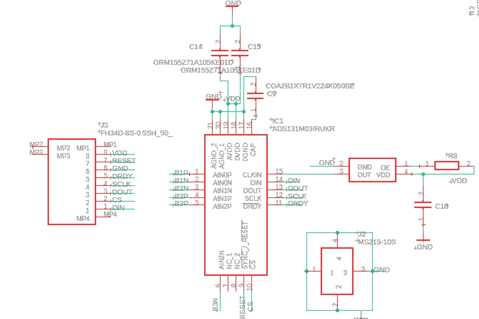
The Schematic is attached: 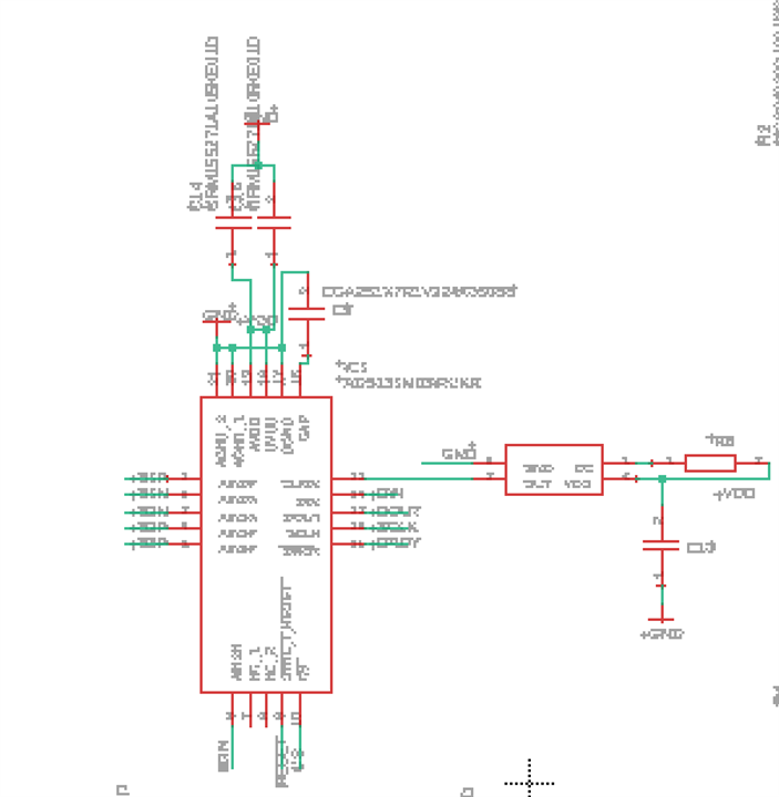
Looking forward to have your suggestion!
Best regards,
Zeyu