This thread has been locked.

If you have a related question, please click the "Ask a related question" button in the top right corner. The newly created question will be automatically linked to this question.

AMC7812EVM-PDK: Can I use without SDM-USB-DIG?

Part Number: AMC7812EVM-PDK

I am attempting to use the AMC7812EVM-PDK without utilizing the provided SDM-USB-DIG for two reasons. 

1. I am sending SPI frames to the device with an esp32-s3 via the test points. 

2. I could not get the software to work correctly and interface with the SDM-USB-DIG on my windows 10 machine. 


Can I use the evaluation module without using the SDM-USB-DIG?
I am routing 3.3V into pin 3 on connector J6.
I moved jumper JP5 to 2-3.  
I have pin 4 on connector J6 tied to ground. 
I have a 24V power supply connected to J5. 
D2 and D3 are lit up. 

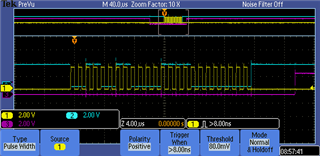
I'm sending SPI frames, 24 clock cycles long, 24 bits long, into the data line (TP6). 

My most significant bits, Bits[23-16], are 10110011, corresponding to B3 in hex, which should write to register 33, the DAC0 register. 

Is what I am doing going to work on the EVM? I am not getting an output on the DAC0 pin on J2, and I am wondering why?

  • Hi Garth,

    If you are able to see SPI pulses on an oscilloscope, then you should be able to communicate with the part. That would be the first thing I would check.

    In addition:
    You're sending data into TP6 (SDI), but are you controlling the other SPI pins? TP7 (SCLK) should be getting a clock signal, and TP8 (CS) should be held low for writing.

    DAC0 register address is 0x33, not 0xB3. By writing 0xB3 as your [23-16] bits, you're actually setting the part in read mode. For writing via SPI, make sure Bit 23 is 0. Your initial writing should be 00110011 for DAC0 register.

    Let me know if this works for you.

    Thanks,
    Erin

  • Thank you Erin. 
    I have SCLK on TP7, and I have CS on TP8 held low for writing. I have also connected SPI pin 12 which connects to the DIG connector (J1) to my terminal block (J6) pin 3, to bring it high to put it into SPI mode. This essentially connects it to IOVdd, which is what the datasheet calls for to put it into SPI mode. 

    After changing the first bit to 0. I am still not reading anything from DAC0. 
    I am sending: 0x330F00 according to my digital scope. 

  • Hi Garth,

    JP1 should be connecting DIG_GPIO6 to IOVDD with its default jumper configuration, unless you removed the jumper. If you're manually wiring J1 pin 10 to IOVDD, it may be best to remove the JP1 jumper. 

    My next suggestion would be to look at the timing diagrams on page 12 and 13, and make sure your SPI timing falls within the specs. 

    Could you also check the voltage on the REF-OUT pin? This is pin 1 on JP2. This voltage should be 2.5V, and it's required to set the DAC output. 

    Thanks,
    Erin

  • I just checked REF-OUT pin and was getting 0V. So I checked pin 5 on JP2 and was getting a 2.49V there, so I moved the jumper to 5-6 position to get the REF DAC set. 

    I see that IOVDD is 2.49V without my 3.3V input. So I can safely remove my 3.3V and leave the jumper where it is. 

    I will upload a picture (if i can) of my oscilloscope to show you the signal I am sending it currently, as I have inspected the timing diagrams, but will check them again. 

    Thank you for your responses. 


  • Here is the signal I'm currently sending on repeat. 
    Yellow: CLOCK
    Blue: DATA
    Purple: *CS

  • Hi Garth,

    THe 2.49V is a bit low for IOVDD. You should continue to apply the 3.3V IOVDD, especially if that's the voltage range you're using for SPI.

    The Ref Out pin being 0V means the chip might not be receiving power correctly. Could you measure the voltage on TP3 (AVDD/DVDD), TP4 (AVCC), and TP3 (IOVDD) to make sure they're being powered correctly? Also let me know how the jumpers are situated. If you're using the 24V supply, JP3 should be 1~2, JP4 should be 1~2, and JP5 can be any configuation. (1~2 if you're using the 24V, or 2~3 if you want to use a different external supply)

    Thanks,
    Erin

  • TP3 (AVDD/DVDD): 5.028V
    TP4 (AVCC): 13.96V
    TP5 (IOVDD): 3.302V (after replacing the 3.3V signal and removing JP1)

    JP3: 1-2
    JP4: 1-2
    JP5: 2-3

    Thank you Erin. 

  • Maybe I have a defective board or defective chip on board?

  • Alright, those voltages look good.

    I found an additional bit you need to enable. Register Address 6B (Power-Down Register in the datasheet) bit 12. This bit enables the DAC0 buffer. If you enable this bit, the DAC will turn on.

    Are you able to read back from the part, by chance? That would help in knowing if the bits are actually being written.

    Thanks,
    Erin

  • Thank you Erin, I was wondering about the buffer, I will check that register and bit-12 out. I cannot read back from the part at the moment. If my SDM-USB-DIG software worked, then I imagine I could, but I guess that is another story for another ticket. 

  • I sent 0x6b and 0x800 several times, and followed it up with my 0x33 0xF00 to no avail. And of course these are in one frame. Thank you for your help Erin. 

  • I think I should actually be sending to address 0x6b and data 0x1000

  • Hi Garth,

    Yeah, I was just about to suggest that. 0x1000 would be DAC0.

    Oh, another way to tell if you're writing correctly, you can try enabling the internal reference. That's in the same register as 0x6B, bit 13. So perhaps try writing 0x6B 0x3000 and measure the voltage on the REFOUT pin and DAC0.

    Thanks,
    Erin

  • Good idea. Thank you. 

  • Erin, I am getting output on DAC0. Thank you so much for your help. Have a wonderful rest of your day. 

  • Great! Glad things are working now. Have a wonderful rest of your day as well.