This thread has been locked.

If you have a related question, please click the "Ask a related question" button in the top right corner. The newly created question will be automatically linked to this question.

ADC12DJ3200: JMODE1 data stitching issue

Part Number: ADC12DJ3200

Hi team,

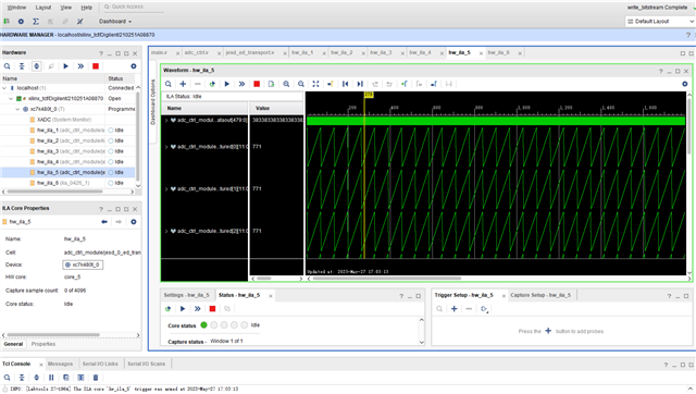
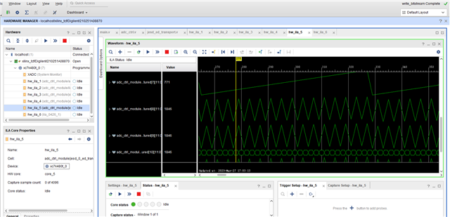
Set ADC to JMODE1 mode, lane_rate=6.4G, K=4, jesd204B_core lck=160MHz, Sysref is 20 MHz, sampling at 3.2 GHz, setting the ramp test mode. Checking the data through ILA, an error occurs starting with the ninth data, as shown in the following figure:
The following figure shows the data resolution:
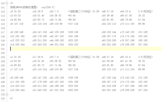
Could you help check this case? Thanks.

Best Regards,

Cherry

  • Hi Cherry,

    I wasn't able to understand the error. Please confirm if you are using 2 Xilinx JESD IP's of 8 lanes each. In that case, each IP will generate an output of 256 bits. The ramp test pattern mode generates an octet ramp (8 bit values), not a sample value ramp (which would be a ramp of 12 bit values).

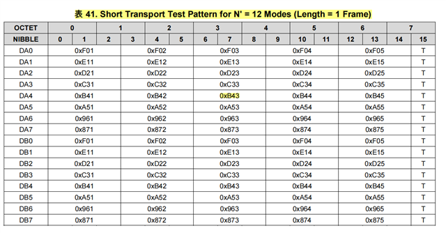
    I will recommend setting the ADC to transport layer test pattern mode. That will make it easy to understand how the lane data is mapped to samples, as there is a constant 12 bit value for each sample in a frame. This value can be found in the 'Short Transport Test Pattern for N' = 12 Modes' table 41 of the datasheet.

    Regards,

    Ameet

  • Hi Ameet,

    Thanks for your support.

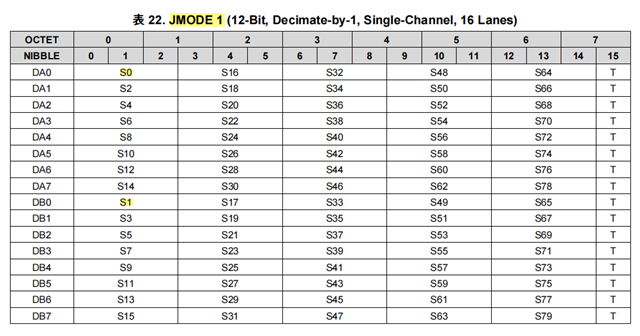
    The customer is currently using transport layer to test pattern patterns. Are the sample points in the order of S0,S1,S2-->S78,S79 of JMODE1? 

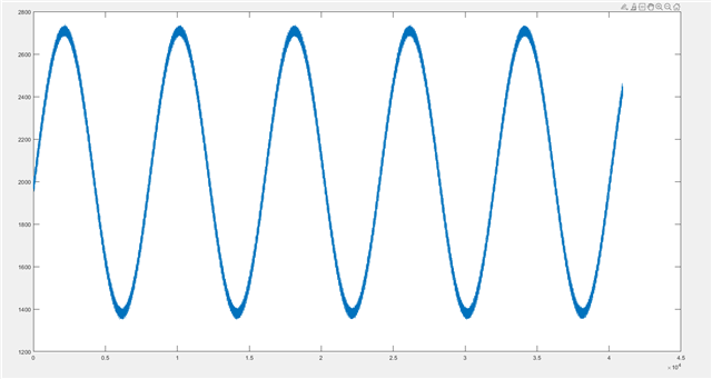
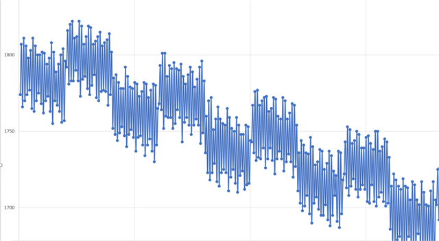
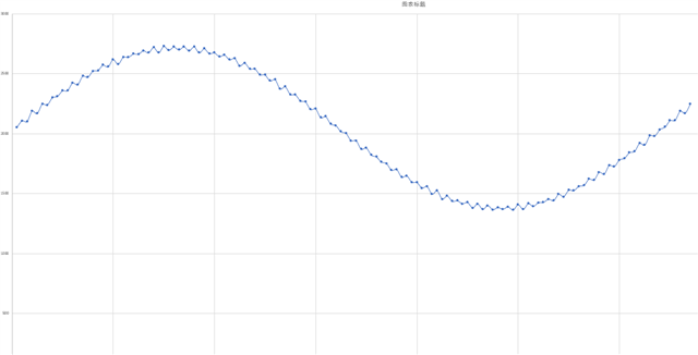
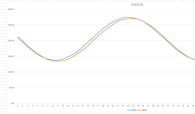
    Also, at use, the first plot below is a sampling of a 100-MHz sine wave, but with a serrated spur. The second plot is the zoomed-in detail. What might be the possible cause of this?

    Thanks and regards,

    Cherry

  • Hi Cherry,

    The ‘transport layer test’ mode is a special test pattern mode of the ADC. Kindly request the customer to configure the ADC in this mode and generate the results of S0-S70. This will give a better idea of what might be causing the issue. 

    I will also request for the RTL code of the transport layer (where lane data is mapped to samples). 

    Regards,

    Ameet 

  • Hi Ameet,

    The image above is a customer generated image using the Transport Layer Test mode, which is fine, but it will fluctuate when sampling sine waves. 

    Currently using JMODE1, with 2 IP cores in the FPGA, the mapping from 256-bit data output from the IP core of the FPGA to samples is divided into: 

    jesd204_0_example_design_1 -> out_data[256:0]  ->S0,S2,S4.......S76,S78

    jesd204_0_example_design_2 -> out_data_2[256:0]  ->S1,S3,S5.....S77,S79

    Thanks and regards,

    Cherry

  • Hi Cherry,

    Unfortunately, the waveforms don’t offer the necessary information to help debug the issue. Kindly send me the following (with the ADC in transport layer test mode):

    1) The exact value on the 256 bit buses (for two consecutive clock cycles)

    2) The customer code for mapping the 256 bit lane data to sample values. 

    Regards,

    Ameet

  • Hi Ameet,

    Thank you and the customer checked the device manual and found that there was a problem with one of the previous settings. A more normal sample is now available, but there are still problems: 

    The figure above shows some sample points, which look like they are alternating and fluctuating, and it seems that the calibration of the sample is not done properly. The current calibration configuration is as follows: 

    0:dout<=24'h0000B0; ///***///Delay of 100 ms after soft reset 
    
    //时钟50MHz 20ns * 5000 = 100 ms
    
    5001: dout<=24'h020000; ///***///Clear JESD_EN (always before CAL_EN) 
    5002: dout<=24'h006100; ///***///Clear CAL_EN (always after JESD_EN) 
    
    
    5003:dout<=24'h020101;//jmode
    5004:dout<=24'h020203;//km
    5005:dout<=24'h020301; //Non-zero means soft synchronization 
    5006:dout<=24'h020400; //00 01
    5007:dout<=24'h020500; //Set JTest 
    
    5008:dout<=24'h0030FF; //Set the range 
    5009:dout<=24'h0031FF;
    5010:dout<=24'h0032FF;
    5011:dout<=24'h0033FF;
    
    5012:dout<=24'h002920;
    5013:dout<=24'h002960;
    
    5014:dout<=24'h002970; //////Set SYSREF_SEL to 0 and use SYSREF calibration 
    
    
    5015:dout<=24'h02B104; //Sets the SRC calibration parameters 
    5016:dout<=24'h02B001; //enable SRC_EN
    
    //5016:dout<=24'h004803; //Set the serializer pre-emphasis to 3 
    
    
    5021:dout<=24'h006201; //Use the foreground calibration 
    
    
    5137:dout<=24'h02C11F; //Alarm Status Register
    5138:dout<=24'h02C200; //Alarm Mask Register
    
    
    5139: dout<=24'h006101; ///***///Set CAL_EN (always before JESD_EN) 
    5140: dout<=24'h020001; ///***///Set JESD_EN (always after CAL_EN) 
    
    
    5141: dout<=24'h006B00; //Setup uses the Calibration Software Trigger 
    
    5142: dout<=24'h006C00; ///***///Set CAL_soft_trig low to reset the calibration state machine 
    5143: dout<=24'h006C01; ///***///Set CAL_soft_trig high to enable calibration, 

    Currently 0X02C/02D/02E registers read C1/00/86, respectively. In the device manual, Table 7. Examples of SYSREF_POS Readings and SYSREF_SEL selections, there is no corresponding mapping of SYSREF_POS[23:0] and OPTIMAL SYSREF_SEL SETTING.

    Currently 0X2B2/2B3/2B4 registers read 15/4D/02, respectively, indicating the SRC_done is not complete. The 0X06A register now reads 08, indicating FG_done is never completed.

    Why's this? Is there a configuration code for the corresponding automatic foreground calibration? 

    The data currently output by the two sub ADCs for ADC12DJ3200 are as follows:

    It should be the calibration issue.

    Thanks and regards,

    Cherry

  • Hi,

    May I know is there any updates?

    Thanks and regards,

    Cherry

  • Hi,

    The customer are still facing the issue and could you help check it?

    Thanks and regards,

    Cherry

  • Hi Cherry,

    Here are the updated register writes. 

    SCR_Done does not complete means the sysref is not getting calibrated properly. Can you please make sure the sysref is getting to the ADC?

    Regards,

    Neeraj