This thread has been locked.

If you have a related question, please click the "Ask a related question" button in the top right corner. The newly created question will be automatically linked to this question.

ADS1258: noise, ground and muxout buffering as single ended

Part Number: ADS1258

Hi,

several questions on this device:

1. is there a requirement of analog and digital GROUND separation between inputs, Anolog supplies , digital supllies?

2. in the datasheet its mentioned that input supply noise should be less than 2mV. is this valid if I want to use the ADC in 16bit (removing the 8 LSBs to remove some noise)? what is the requirement for VREF noise and AVDD noise (single LDO connected to both VREF and AVDD) in this case?

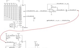
3. using the device in single ended mode, i thought connecting the MUXOUTN to 10K pulldown resistor and the MUXOUTP to unit gain buffer with serial 10K resistor in the positive input, and 10K resistor in the feedback (op amp LTC2054HV). the output of the opamp will be connected to the ADCINP, and the ADCINN will be connected to GND (cap 2.2nF between those inputs). can I use this configuration? 

  • Hi assaf matia,

    Here are the answers to your questions:

    is there a requirement of analog and digital GROUND separation between inputs, Anolog supplies , digital supllies?

    No, in fact it is recommended to have a solid ground plane, and then connect both analog and digital ground to this solid plane.

    in the datasheet its mentioned that input supply noise should be less than 2mV. is this valid if I want to use the ADC in 16bit (removing the 8 LSBs to remove some noise)? what is the requirement for VREF noise and AVDD noise (single LDO connected to both VREF and AVDD) in this case?

    This is a recommendation to keep the power-supply noise at a lower level compared to the ADC noise. So if you are using a 16-bit ADC then having a little more power supply noise might be acceptable. But this is really for you to decide if that is okay for your system

    The VREF noise should be less than the ADC noise, where possible. If not, the VREF noise will dominate the overall noise budget, assuming your signal range extends close to full scale

    using the device in single ended mode, i thought connecting the MUXOUTN to 10K pulldown resistor and the MUXOUTP to unit gain buffer with serial 10K resistor in the positive input, and 10K resistor in the feedback (op amp LTC2054HV). the output of the opamp will be connected to the ADCINP, and the ADCINN will be connected to GND (cap 2.2nF between those inputs). can I use this configuration? 

    Can you draw this configuration, instead of describing it? I would like to see what you intend to do.

    -Bryan

  • Hi,

    thank you for the reply/ regarding your notes:

    1. I meant if before connecting to the solid ground plane should I make a local AGND and local DGND and then connect them to one solid plane using vias?

    2. so if I understood correctly if the reference noise is for example 10mV , I will have 10mV noise at the readings, since no noise rejection in the reference input?

    3. attached the schematic as you asked.

    thank you!!!

  • Hi assaf matia,

    1. I meant if before connecting to the solid ground plane should I make a local AGND and local DGND and then connect them to one solid plane using vias?

    I'm not sure what this means. If all of the ground connection points are connecting to a solid ground plane, then why would have you AGND and DGND? They should all be at the same potential, so unless you want to have different net names to distinguish between analog and digital ground points, I think this would be more confusing than anything else

    so if I understood correctly if the reference noise is for example 10mV , I will have 10mV noise at the readings, since no noise rejection in the reference input?

    VREF noise scales with input signal, so the answer to this question is not so simple. I would encourage you to review the "ADC noise" videos in our Precision Labs training content. There is a lot to consider regarding how noise affects your measurement, and it is more than I can communicate in this e2e thread: https://www.ti.com/video/series/analog-to-digital-converters-adcs.html

    attached the schematic as you asked.

    Instead of using the system you have shown and grounding ADCINN, you could potentially tie AINCOM to a mid-supply voltage e.g. 2.5V. Then you would measure your single-ended signal on AINx (e.g. AIN9) with respect to this voltage, instead of ground. You could then buffer both MUXOUTP and MUXOUTN. This is called a pseudo differential measurement. It will allow you to use more of the ADC's code range because the ADC's code range is bipolar. Right now, with a single-ended signal and ADCINN grounded, you can only use half of the ADC's code range (0 to +FS)

    -Bryan