This thread has been locked.

If you have a related question, please click the "Ask a related question" button in the top right corner. The newly created question will be automatically linked to this question.

ADS131M08: ADS131M08

Part Number: ADS131M08
Other Parts Discussed in Thread: ADS131M04, ADS131M03

Hi,

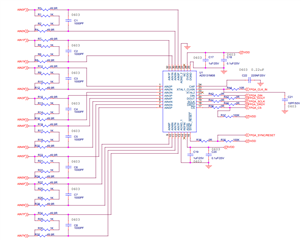
Right now, I'm using ADS131M08 for new design. Load cell direct connect to our ADC. I have noise level is high without connecting load cell. how to reduce the input noise level.

Input resistance is 49.9 ohm and common mode capacitor is 1000PF.

  • Hi Ponraj,

    It will be helpful if you could share your schematic, explain your ADC configuration (gain, data rate and so on) and also let me know how much noise you got.

    Regards,

    Dale

  • Hi Dale Li,

       Thanks, for your reply. My ADC configuration mentioned as below. 

    Clk - 8.1818MHz (From FPGA), SCLK - 20MHz, Gain - 128, Data rate - 8KHz, Internal reference

    Datasheet says 13.4 bits resolution, but we get 10 bits. 

    1K + 1K use for loaded resistor.

    Previously we worked with ADS131M04, but we get resolution as per the datasheet. If any changes between these two devices.

  • Hi Ponraj,

    Please see my feedback below:

    • When you measure the noise and check effective resolution, the input of ADC should be shorted. You can write 01 to MUXn[1:0] to get the RMS noise, then calculate the effective resolution.
    • If you do not short the input on the ADC, you are actually measuring noise not only from the ADC, but also from your external circuity including noise caused by pcb layout and so on.
    • Common-mode capacitors between inputs and AGND are helpful for your design.
    • There is no difference between M08 and M04 in terms of the noise and effective resolution spec under your configuration condition.

    Best regards,

    Dale

  • Hi Dale Li,

        Thanks for your reply. I checked with above 1st points, Gain = 128, SPI clock = 20MHz and ADC input pins shorted, i get 10 bit resolution. so i change my SPI clock only ,Gain = 128, SPI clock = 10MHz and ADC input pins shorted, i get 13 bit resolution. 

    When i connect with my strain bridge voltage, i get 10 bit resolution, how to improve my resolution?

    I change and check the ADC input filter frequency, but that changes won't help us.

  • Hi Ponraj,

    This M08 ADC supports SCLK frequency up to 25MHz when DVDD is 3.3V. Your 20Mhz SCLK might not be very clean, it depends on your clock source, the length of your trace and you pcb layout. You can try to use a small resistor value for R41, e.g. 49.9ohm instead of 0ohm.

    I did not know how you excited your bridge, how you connected it and what is your signal level, however a ratiometric measurement should be typically configured for bridge application. The ratiometric measurement is less susceptible to any Vexcitation drift over time and temperature and also any noise from the Vexcitation source will be cancelled out assuming that the noise at the reference input and the measurement input are correlated. See more details in the application note below:

    A Basic Guide to Bridge Measurements

    Regards,

    Dale 

  • Hi Dale Li,

    suggest to below observation.

     1. When we apply 4 gains then i get the resolution as per the datasheet and when we apply 128 gains with same sensor (bridge) we are not getting resolution as per the datasheet and along with glitches in MIN & Max noise level. We are using 350-ohm bridge sensors.

    2. we are trying to internal and external ref voltage. We are getting glitches only in internal voltage using. External ref voltage is fine.

    3. What is max level of external voltage?

  • Hi Ponraj,

    Please see my response below:

    1. The noise(or the resolution) in the datasheet only reflects the noise of the device. What you measured reflects your system noise including the noise from the bridge. The noise is amplified too. 

    2. Using an external reference (Vref) with a ratiometric measurement for connecting a bridge to the ADC can usually cancel out any noise from the excitation source (Vexcitation), make your measurement independent of the value of Vref and Vexcitation and also less susceptible to any Vexcitation drift over time and temperature. I strongly recommended you to check A Basic Guide to Bridge Measurements.

    3. The recommended Vref is shown in the table 6.6 of the M08 datasheet: 

    Regards,

    Dale

  • Hi Dale li,

        I need more gain, when my sensor calibration. So, i connect external differential amplifier and then send to ADC input. In my case i get only 14 bits for 4gain and 8KSPS. why I'm not getting resolution as per the datasheet. When i use 128 PGA gain then i get more noise, so i reduce my PGA gain and increased external gain. 


  • Hi Ponraj,

    As I previously said, the noise(or the resolution) in the M08 datasheet only reflects the noise of the device. Based on your description, you are seeing more noise from the external circuit including amplifier and bridge. To check the ADC's noise, you can wite the MUX[1:0] bits of CHx_CFG register to short the ADC input, then check the standard deviation of code.

    When you using large gain on the ADC, everything will be amplified including your higher noise from the external circuit (amplifier and bridge), this is the reason you got more noise at higher gain 128.

    The following recommendations may help you reduce your system noise:

    • Use a clean power supply as the excitation voltage for the  bridge, also use a voltage divider to divide the same power supply to get a 1.2V as the reference REFIN for M08 ADC. A buffer is needed because M08 does not have an internal reference buffer.
    • Use low noise external difference amplifier.

    Regards,

    Dale

  • Hi Dale,

    We are facing an issue as explained below:

    We are connecting the ADC differential inputs with differential output of a load cell (4kN, 5kN, 25kN, 50 kN tried) which has a Wheatstone bridge. We are using the DC supply of 5V. The moment we connect the load cell we have the good resolution i.e. as per datasheet. But, when we calibrate the system using the shunt we are loosing the resolution. And also, we observe that the ADC works without any spikes in the output with gain less than 8, but for higher gain like 128 (which we desire for our system) we get spikes in the output. We tried your suggestions but still failing. We also tried connecting higher shunt (2000 & 1000 ohms instead of 350 ohms) but we are not getting the resolution as per the datasheet. Where are we failing? Do you help us in resolving this?

    The signals SCLK, power supply are clean and observed for long time.

    Regards

    Prakash

  • Hi Prakash,

    I try to help out here while Dale is on travel.

    I read through the whole discussion, but honestly still don't understand how you want to make the system work at all.
    My understanding is that you are using a Wheatstone bridge which is excited with 5V. The ADS131M03 is supplied with 3.3V.
    In this case the common-mode output voltage of the bridge sits at 2.5V. If you connect the sense lines of the bridge directly to the ADS131M08 inputs, your system will not work for gains >= 8.
    The datasheet states in the Recommended Operating Conditions table, that your absolute input voltages on each pin need to be <= (AVDD - 1.8V) = (3.3V - 1.8V) = 1.5V for gains >= 8. In your case the absolute voltages are at 2.5V though.

    You have a few options to make the system work with ADS131M08:

    • Decrease the bridge excitation voltage to <=3V
    • Use a bipolar supply, e.g. +/-2.5V, as the bridge excitation
    • Use an external instrumentation amplifier to gain up the signal and level shift it to within the input range of the ADC.

    Another question I would have is, how do you determine/calculate the resolution you are getting?

    Regards,
    Joachim Wuerker

  • Hi Joachim,

    Thanks for the response.

    I am interested in connecting a load cell of any capacity and meet the resolution as per the datasheet, i.e., without varying the load cell but connected to differential input I should be having very low noise.

    Yes. My load cell is excited with 5 V DC.

    Will try decreasing the excitation and check. We are not permitted to for bipolar excitation. Will try also the instrumentation amplifier along with level shifter and let you on the same.

    Roughly calculate the noise level with (1/2^N) *100%, where N is the number of resolution bits. It will be closer but not exact.

    Will try your suggestions and let you know.

    Regards

    Prakash

  • Hi Prakash,

    sounds good.
    When using an INA, the INA will do the level shifting for you typically.

    You might have a wrong expectation when it comes to the resolution you will be able to achieve.
    If you want to know if you can achieve the datasheet noise performance when the ADS131M08 is connected to the load cell, you would have to keep the load cell close to 0V differential output voltage. Then record a number of samples, e.g. over a period of 1ms. Plot the codes over time to make sure there is no drift or other disturbance in it. The standard deviation of the recorded codes is then considered the rms value of the codes. Now convert the rms code value to uV using the LSB size. The measured uVrms value should then be close to the value stated in the datasheet noise table for the given gain and data rate setting.

    Regards,
    Joachim Wuerker