This thread has been locked.

If you have a related question, please click the "Ask a related question" button in the top right corner. The newly created question will be automatically linked to this question.

ADS114S08: Quesions on Noise Performance of ADS114S08

Part Number: ADS114S08
Other Parts Discussed in Thread: ADS124S08, REF6225

Dear TI Experts,

  I have two questions regarding noise performance in ADS114S08 datasheet.

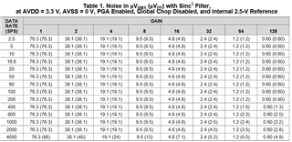
  1.  The following table is noise performance in terms of uVrms and uVpp.  I understand we use RMS and peak-to-peak noise voltage to calculate effective and noise free resolution, respectively.  However, How do we get RMS noise = p-p value in some scenario, instead of something like RMS noise x (square root 2) = p-p noise value in the case of a sine wave?
2. In what scenario do we prefer to use an external amplifier circuit, rather than using PGA gain? Specifically, if we want to have a gain of 8, is there any reason we may not choose to leverage internal pga gain?

I've thought of one and not sure about it. If we apply negative voltage supply for pga, i imagine it has also to be a really stable negative voltage reference as internal reference is not used.  Is that right?

Would appreciate your help.

Regards,

Yuanchen Zhu

  • Hi Yuanchen Zhu,

    Answers to your questions:

    The following table is noise performance in terms of uVrms and uVpp.  I understand we use RMS and peak-to-peak noise voltage to calculate effective and noise free resolution, respectively.  However, How do we get RMS noise = p-p value in some scenario, instead of something like RMS noise x (square root 2) = p-p noise value in the case of a sine wave?

    In this case, the noise is limited by the ADC's LSB size. This is why the RMS and PP are the same for this 16-bit ADC, because there is effectively no difference between the RMS or PP noise. If you look at the 24-bit version of this device (ADS124S08), you will see that the RMS and PP noise are different in all cases, where the PP noise is approximately 4-6x bigger compared to the RMS noise.

    You can review the "ADC Noise" videos in our Precision Labs ADC training content for more information: https://www.ti.com/video/series/analog-to-digital-converters-adcs.html

    In what scenario do we prefer to use an external amplifier circuit, rather than using PGA gain? Specifically, if we want to have a gain of 8, is there any reason we may not choose to leverage internal pga gain?

    Typically the ADC's integrated PGA will be sufficient for most applications. You might choose an external amplifier when you need to measure high voltage signals e.g. +10V, which is not inherently supported by the ADS114S08.

    I've thought of one and not sure about it. If we apply negative voltage supply for pga, i imagine it has also to be a really stable negative voltage reference as internal reference is not used.  Is that right?

    Both supplies (AVSS and AVSS) should be stable in a bipolar application. And I'm not sure what this has to do with using the ADC internal reference.

    -Bryan

  • You might choose an external amplifier when you need to measure high voltage signals e.g. +10V, which is not inherently supported by the ADS114S08.

    Hello,Bryan. I understand that now.

    And If we stick to use ADS114S08, if we have a high voltage signal, e.g. +10V as you said, can I take from you that we need an external amplifier to actually attenuate the signal with a gain of less than 1 to make the resulting range fall into ADS114S08 voltage spec?

    Both supplies (AVSS and AVSS) should be stable in a bipolar application. And I'm not sure what this has to do with using the ADC internal reference.

    Sorry for being vague with the word "stable". First , let me clarify a bit more the scenario in my mind. suppose we have a differential input and an external differential amplifier that is supplied with +Vcc and -Vcc (from charge pump), In the first way, i suppose we can leverage the internal reference voltage Vref(2.5V) to put middle bias at a right level, which means we don't need a negative voltage for VSS or REFN pin of ADC.

    Previously, I meant for +Vcc and -Vcc we need "a stable voltage" with as low noise or ripple as possible to have good accuracy , but not necessary of high precision (e.g. difference between stable 3.3V and stable 3.35V matters little here).

    In contrast, as I understand if we use +Vcc and -Vcc for REFP and REFN of ADS114S08, both voltages need to have high precision(which I thought is more strict than "a stable voltage", it needs to be a precise voltage as we presume), maybe from voltage reference. (How to get a precise negative voltage is not intuitive to me right now).  Anyway, based on this case, I am not sure for the following things: to use internal pga, I suppose we don't usually use same source for AVDD(AVSS) and REFP(REFN)? And this is where I think we may need to take care of both the voltage supply(+ and -) and reference voltage (+ and -), which i think may takes a bit effort.

    Please don't hesitate point out and correct me if I have any stupid statement.  And do we have a reference design for this scenario from TI? Or any suggestion? Would really appreciate your help.

    Regards,

    Yuanchen

  • Hi Yuanchen Zhu,

    My comments below

    And If we stick to use ADS114S08, if we have a high voltage signal, e.g. +10V as you said, can I take from you that we need an external amplifier to actually attenuate the signal with a gain of less than 1 to make the resulting range fall into ADS114S08 voltage spec?

    Yes, exactly. You cannot apply 10V directly to the ADS114S08, so you would need to attenuate this voltage into the input range of the ADC. This would be necessary for Analog Input modules in PLC systems where you need to measure +/-10V process inputs

    Previously, I meant for +Vcc and -Vcc we need "a stable voltage" with as low noise or ripple as possible to have good accuracy , but not necessary of high precision (e.g. difference between stable 3.3V and stable 3.35V matters little here).

    This is generally true. The ADS114S08 for example can support an AVDD voltage of 2.7V to 5.25V, so as long as the voltage is within this range you can expect performance as defined in the Electrical Characteristics table. However, the voltage of AVDD and AVSS directly impact the allowable input voltage (see Table 7.3), so this is something else to consider

    In contrast, as I understand if we use +Vcc and -Vcc for REFP and REFN of ADS114S08, both voltages need to have high precision(which I thought is more strict than "a stable voltage", it needs to be a precise voltage as we presume), maybe from voltage reference.

    Yes, the voltage at REFP and REFN is what the ADC uses as a reference voltage, and therefore must be both accurate and precise. Using a discrete voltage reference, or the ADC's internal reference voltage, is the best choice. Unless you use a sensor such as an RTD or a load cell where the reference voltage can be ratiometric and is therefore generated by the sensor excitation voltage

    (How to get a precise negative voltage is not intuitive to me right now).  Anyway, based on this case, I am not sure for the following things: to use internal pga, I suppose we don't usually use same source for AVDD(AVSS) and REFP(REFN)?

    If you are going to use a discrete VREF or the ADC's internal VREF, REFN should be tied to AVSS. Then, the GND pin on the discrete VREF should also be tied to AVSS, or if you use the internal VREF it is internally connected to AVSS. In this configuration the reference voltage is always relative to AVSS, so even if AVSS shifts a little, the differential reference voltage is stable and accurate.

    Unless you are trying to measure signals >AVDD with your system, or the common-mode range of the ADC internal PGA is insufficient, I am not sure why you would need the difference amplifier. Can you help me understand what signals you are trying to measure, and why the internal PGA will not work in this case?

    -Bryan

  • If you are going to use a discrete VREF or the ADC's internal VREF, REFN should be tied to AVSS. Then, the GND pin on the discrete VREF should also be tied to AVSS, or if you use the internal VREF it is internally connected to AVSS. In this configuration the reference voltage is always relative to AVSS, so even if AVSS shifts a little, the differential reference voltage is stable and accurate.

    Hi, Bryan

      I understand now. I thought we need a precise negative voltage which is tied to REFN for a differential input signal, and thus I thought using an external amplifier topology with bias voltage free me from doing this.

    Understand the method that we can connect GND pin on discrete VREF to AVSS ( and REFN), since what we always need is a differential reference voltage. My question is perfectly solved.

    Really appreciate your explaination.

    Regards,

    Yuanchen

  • Hi Yuanchen Zhu,

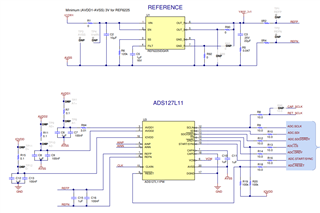
    As an example, the image below is taken from the ADS127L11EVM (https://www.ti.com/tool/ADS127L11EVM). You can see how the REF6225 is connected for this device to REFP/REFN, and that REFN is connected to AVSS, as are the REF6225 GND pins (pin 7 and 8).

    I hope this helps provide an example of how a precision VREF is connected to an ADC. Or, as mentioned previously, you can use the ADC's internal VREF which will be connected to AVSS internal to the device

    -Bryan