Part Number: ADC3662
Other Parts Discussed in Thread: THS4541
In adc3662`s datasheet, chapter 6.6 say that input full scale is 3.2 Vpp and input commom model voltage is 0.95V. So the input range is from (0.95-1.6)V to (0.95+1.6)V. Is it right? However, chapter 6.1 the absolute maximum ratings, limit the ainp and ainm from -0.3V to 2.1V?
In chapter 9.1.1:
" When designing the amplifier/filter driving circuit, the ADC input full-scale voltage needs to be taken into
consideration. For example, the ADC366x input full-scale is 3.2Vpp. When factoring in ~ 1 dB for insertion loss
of the filter, then the amplifier needs to deliver close to 3.6Vpp. The amplifier distortion performance will degrade
with a larger output swing and considering the ADC common mode input voltage the amplifier may not be able to
deliver the full swing. The ADC366x provides an output common mode voltage of 0.95V and the THS4541 for
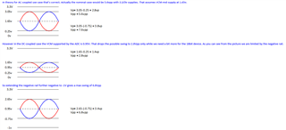
example can only swing within 250 mV of its negative supply. A unipolar 3.3 V amplifier power supply will thus
limit the maximum voltage swing to ~ 2.8Vpp. Hence if a larger output swing is required (factoring in filter
insertion loss) then a negative supply for the amplifier is needed in order to eliminate that limitation. Additionally
input voltage protection diodes may be needed to protect the ADC from over-voltage events."
Output voltage swing of THS4541 vs power supply
DEVICE MIN OUTPUT VOLTAGE MAX SWING WITH 3.3 V/ 0 V SUPPLY MAX SWING WITH 3.3 V/ -1.0 V SUPPLY
THS4541 VS- + 250 mV 2.8 Vpp 6.8 Vpp
When a single 3.3V supply for THS4541, output is calculated as 3.3V-0V-2*0.25V=2.8Vpp
So when supplied with a 3.3V and a -1.0V, output should be calculated as 3.3V+1V-2*0.25V=3.8Vpp, why is 6.8Vpp. Am I wrong in understanding the THS4541?


