Because of the holidays, TI E2E™ design support forum responses will be delayed from Dec. 25 through Jan. 2. Thank you for your patience.

This thread has been locked.

If you have a related question, please click the "Ask a related question" button in the top right corner. The newly created question will be automatically linked to this question.

DAC5688: PLL CLOCK MODE

Part Number: DAC5688
Other Parts Discussed in Thread: DAC5687, DAC5686

Hi

Im using the DAC5688 in PLL clock mode with CLK1 = 250 MHz and CLK2 = 250 MHz and the Frequency desired on PLL is 500 MHz (intp x2). For that M = 4 and N = 2. Sometimes i see a glitch or noise on my sine signal. I have a question about the reference clock for PLL.

If the CLK1 is 250 MHz, the input on PFD its already over the maximu frequency (160 MHz) ? or this parameter is for the feedback.
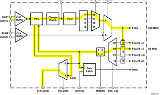

This block diagram is from the next application note : https://www.ti.com/lit/an/slwa040a/slwa040a.pdf. There is mencionated that the CLK2 its not used for DAC5686 and DAC5687. Its the same case for the DAC5688 ? 

Regards,

Juan Camilo Peña

  • Juan,

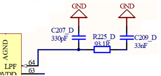
    CLK2 is required when using the DAC in PLL mode. This is the reference clock. The PFD frequency is CLK2 after going through the N divider. In your case, this would be 125MHz, which is less then the max PFD frequency requirement of 160MHz. Your issue may be related to the parts used for the LPF. Go to the DAC5688 product folder on the TI website and download the DAC5688 LPF calculator to assist with part selection for your filter. Also suggest setting your PLL_gain = '10' and PLL_range = '0011' per the data sheet with the VCO running at 500MHz. 

    Regards,

    Jim

  • Hi Jim, thanks for your answer.

    Im going to look the LPF calculator, actually we have the EVM design.

    This is our DAC outputs and measured with an oscilloscope  (CHA = yellow, CHB = purple) 

    Sometimes, when we changed the frequency on CHB, the CHA looks noisy take a look to the next image.

    To fix it, we are synchronizing the FIFO through the SYNC pin (CONFIG 23 -> 0x08) and this solve the issue aparently, so, we are synchronizing the FIFO every time we change the frequency for both channels but we dont think this is the best solution.

    Thanks and regards.

    Juan Camilo Peña A.

  • Hey Juan, 

    Are you currently just using the NCO to generate these tones or are you sending a digitized sinewave to the DAC via an FPGA? Curious what all is being done when you change the frequency. 

    Regards, 

    Matt

  • Hi Matt,

    We are using a FPGA to generate digitized waves and we are monitoring these FPGA outputs trought an ILA and it shows the signals without noise.

    Regards,

    Juan Camilo Peña A.

  • Hey Juan, 

    So just to be clear, only the input data to the DAC is changing when the frequency is being updated. The DAC itself is not having any of its registers modified and you're seeing this behavior when changing the input data stream to have a different frequency generated at the output of the DAC.

    Regards, 

    Matt

  • Yes Matt, the DAC its not changing any register.

    This is the Register map configuration:

     0x01 0x0D //CONFIG1
    0x02 0x48 //CONFIG2
    0x03 0x00 //CONFIG3
    0x04 0x00 //CONFIG4
    0x05 0x90 //CONFIG5
    0x06 0x00 //CONFIG6
    0x07 0x00 //CONFIG7
    0x08 0x00 //CONFIG8
    0x09 0x00 //CONFIG9
    0x0A 0x00 //CONFIG10
    0x0B 0x20 //CONFIG11
    0x0C 0xA6 //CONFIG12
    0x0D 0xA6 //CONFIG13
    0x0E 0x00 //CONFIG14
    0x0F 0x2D //CONFIG15
    0x10 0x00 //CONFIG16
    0x11 0x00 //CONFIG17
    0x12 0x00 //CONFIG18
    0x13 0x00 //CONFIG19
    0x14 0x00 //CONFIG20
    0x15 0x00 //CONFIG21
    0x16 0x00 //CONFIG22
    0x17 0x08 //CONFIG23
    0x18 0x80 //CONFIG24
    0x19 0x00 //CONFIG25
    0x1A 0x0D //CONFIG26
    0x1B 0xFF //CONFIG27
    0x1C 0x00 //CONFIG28
    0x1D 0x19 //CONFIG29
    0x1E 0x13 //CONFIG30
  • Hi Juan,

    This is a strange one. When you change channel B incoming data, then channel A waveform looks distorted until a FIFO sync is issued, am I understanding this correct?

    How are you changing the input signal to the DAC? I understand this is through ILA but are you dropping any samples prior to the signal change? This would cause the FIFO needing to be re-synced if some samples are dropped. If this is the case, can you try with the initial output signal and then embed the new signal in a manner where no samples are dropped and see if issue persists?

    What is the initial output frequency and what is the new output frequency you change to when this issue occurs?

    Thanks, Chase

  • Hi Chase,

    1. Yes, when we updated the CHB frequency, the CHA works correctly most of the time. Eventually and randomly the change of CHB frequency cause a distortion on CHA waveform and for now just the FIFO sync fix this problem.

    This is a strange one. When you change channel B incoming data, then channel A waveform looks distorted until a FIFO sync is issued, am I understanding this correct?

    2. The input signals are generated on FPGA, the ILA is only use to verify the correct signal generation on FPGA. In our case when the distortion appears on CHA or the distortion doesnt exist, the signals on the ILA looks correctly. Frequency changes are generated at the frequency we want to have at the output.

    How are you changing the input signal to the DAC? I understand this is through ILA but are you dropping any samples prior to the signal change?

    3. What do you mean with this ? 

    If this is the case, can you try with the initial output signal and then embed the new signal in a manner where no samples are dropped and see if issue persists?

    4. How I say in the firts answer, the issue occurs randomly. That's why I think it may be the clock mode configuration.

    What is the initial output frequency and what is the new output frequency you change to when this issue occurs?
  • Hey Juan, 

    How are the samples being produced for the DAC? Are they being made in real time or are you loading a waveform in a circular buffer?

    If they are being made in real time how much memory do you have on the FPGA?

    Regards, 

    Matt

  • Hi Matthew,

    The signals are being generated in real time on FPGA (Kintex7), the sampling clock is 250 MHz and this same clock goes to the CLK1 (DAC5688). We dont use memory for save data, each sample (16 bit) is send according to the sampling code.

    Regards,

    Juan C

  • Hey Juan, 

    I would check and see if there is any type of change in timing when you update the frequency on the FPGA. The device should just see samples coming in, regardless of the data that is embedded in the sample stream. 

    Unfortunately I do not have a way to test this with my setup as the FPGA setup I have is not capable of changing samples in real time. The solution you have, while not ideal, appears to fix the issue so I would keep going with that.

    Regards, 

    Matt