Other Parts Discussed in Thread: LMK04828,
Hello,
We now have the board built and are in the process of bringing up.
The schematic was reviewed before but wanted to double check.
- on Sheet 18
- MGTREFCLK0P/N is 160 MHz device clock to the FPGA (receiver)
- FPGACLK1P/N is 8 MHz SYSREF to the FPGA
- ADCCLKP/N is the 160 MHz clock to the ADC (ADC32J25IRGZT, transmitter)
- SYSREFP/N is the SYSREF to the ADC
- Should they be all LVDS?
- If so I should remove R414 and R415
- Should I also update R418 and R419 to 0 Ohm?
- Do I still need R346 and R347 for LVDS going to the FPGA?
- Previously the following was mentioned
- The lane rate = (Fs * 10 * F) / S. With LMFS = 2221, this is (160M * 10 * F) / 1 = 3.2Gbps. If you use a value of 20 for K, your SYSREF = Fs / (N * K), where N is any whole integer. If N = 1, your SYSREF = 8MHz.
-
Per the JESD204B standard, the following two equations must be met:
1 < K < 32
17 < F*K < 1024
Since your F is 2, K will need to be at least 9. The larger value you use for K, the more buffering you provided for the data, but the larger the latency will be. Some parts only allow certain values of K to be used.
- N doesn't seem to be tied to any parameters. Then K becomes arbitrary. How do I determine N?
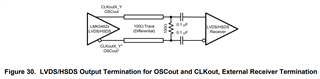
The schematic was reviewed but could you take another look at
- Sheet 2: SYNCP_ADC & SYNCM_ADC
- are generated as 3.3V CMOS
- Sheet 3: FPGACLK1P/N: SYSREF from LMK04828
- LVDS
- Sheet 5: DAP/M_ADC, DBP/M_ADC, and GTREFCLK0P/N
- All LVDS
- Sheet 15: ADC32J25IRGZT
- Sheet 18: LMK04828
I think all of the differential signals are LVDS except SYNCs.
I would appreciate if you could take another look and confirm on the circuits and terminations.
Regards,
Andrew