This thread has been locked.

If you have a related question, please click the "Ask a related question" button in the top right corner. The newly created question will be automatically linked to this question.

ADS8353: ouptut code issues on ADS8353

Part Number: ADS8353

Hi all,

I have an issue on the ADS8353 ADC that I’d like to consult with you or maybe the factory about.  I have been using this chip on other designs for many years and have never encountered this problem. 

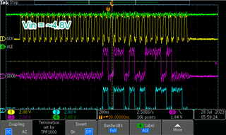
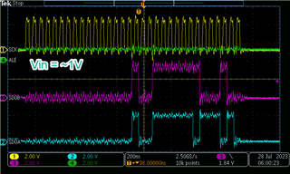
Basically, on some of our channels in one particular design, it looks like the MSB and the second-to-MSB are stuck at 1 and 0, respectively, regardless of what the input to the ADC is.  I believe this always happens on both ADC channels in the chip.  We are operating in 32-clock, dual SDO mode.  AVDD is 5.1V; both references are 5.0V, and DVDD is 3.3V.  I’ve checked all supplies and references on multiple boards, and they look good. 

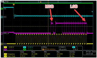
In the following scope plot, I’ve captured the channel A output code when the input to the ADC (green trace) is close to 5V.  You can see the MSB is 1, as expected, but the next-to-MSB is 0, when it should be 1, since it represents the highest quarter of the ADC range. 

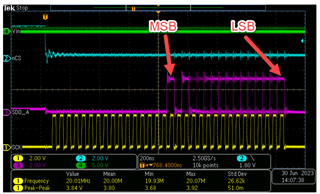
In this plot, I’ve captured the output code when the ADC input (green trace) is close to 0V.  For inputs close to zero, I’d expect that most of the higher weight bits would be zero, but you can see that the MSB and next-to-MSB are the same as they were above, 1 and 0, when they should both be zero in this case.

You can see that those two bits never seem to move.  It’s possible that this is a manufacturing issue, as we have most of the channels working normally.  However, there are larger than expected number of channels that exhibit this same symptom, I’d say maybe 10-20%.  (this is the first that I’ve probed the SPI to see what’s actually going on, but the behavior of the others is consistent.) 

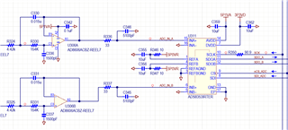
Also including a schematic screen grab of the ADC for reference:


The part markings on this particular ADS8353 specimen are:

8353

TI7A

PD1F


All ADC chips have the same markings, both those that exhibit this behavior and those that don’t.

Off the top of our heads, we’re thinking that maybe we somehow have the mode setup wrong when we’re programming the ADCs, or possibly edgy since most of them work ok?  We are right at the clock spec limit (20MHz) but we’re used these parts for years at 20MHz without ever having seen this.  Possibly a batch of these chips is more sensitive than others to clock frequency?  Any other ideas? 

Thanks in advance, Happy 4th if you're in the US, and look forward to hearing your thoughts!

Geoff

  • Hello Geoff,

    Thank you for your post. We'll take a look at this question after the holiday.

    Regards,

    Ryan

  • sounds good, happy 4th!

  • Hi Geoff,

    Thanks for your patience. Has anything new been learned since your original post?

    This certainly seems like unexpected behavior, especially for input signals near 0V where the MSB should be 0b for straight binary output. Can you confirm the rest of the CFR register settings?

    Also, just for the sake of documenting the issue, can you repeat the above screen captures for SDO_B as well?

    Regards,

    Ryan

  • Hi Ryan,

    Thanks for the reply.  Please give me a couple of days to get back to this; our firmware guy is out of the office, and may not be able to work on this when he gets back due to some other high priority jobs.  

    That being said, we are intending to set CFR.B9 to 0 to use the full 0-5V input range given our 5V reference.  Most of the boards in this design work in this intended manner, with 0~5V input range giving us the full 0-65536 output codes.  So if there is something set wrong in these ~25% of problematic channels, it's possibly an edge case in the firmware or something similar. 

    Similarly, we intend to set B7 to 0 to use the single-ended mode.  

    If these were set wrong, though, would it manifest in this way?

    I'll try to get some measurements on the -B channel as well.

    Thanks

    Geoff

  • Hi Geoff,

    I don't see a way for the device to be misprogrammed and produce the 1b-0b output you are observing in the first two bits. Also, the default value for the CFR register is 00h at startup, so you could test this without any register write commands and expect the same results (0 to VREF range, straight binary format, external reference, etc.). We have reproduced your setup on our EVM and have yet to find any combination of register settings and input voltages which would produce such behavior.

    Looking forward to the results from testing Channel B.

    In addition, if you have a "known good" device which you can use to replace one which exhibits this behavior, that may help to rule out any other edge case scenarios in the firmware.

    Regards,

    Ryan

  • Hi Geoff - any updates here? - Ryan

  • Hi Ryan, my apologies for the dealy.  I've been in the hot seat on another project, unfortunately.  

    I think i will have some cycles to get back to this next week - I appreciate the follow-up, and have a nice weekend!

  • Hi Ryan sorry for the long delay; i have some cycles today and was able to get back to this.  

    1. I do see the same stuck code on the second SDO output, see plots below: 

    (Ignore the ALE label, that's the input voltage! I forgot to rename that channel before I grabbed the picture.)

    I'll try swapping the part as you suggested and see if it goes away.  

    Thanks

  • Thanks for the update, Geoff. Let us know how the part swapping goes. -Ryan