Hi,
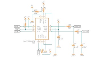
I'm doing a PCB design using DAC7552 and I've designed the PCB according to the following schematic design. Is this correct?

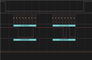
I'm not getting any output from the DAC channels, I didn't use any power down command and directly used the following command in a 16bit data frame through SPI communication.
Power down commands in the datasheet are really confusing, as there are multiple occurrences for the same scenario.

Am I missing something here?


