This thread has been locked.

If you have a related question, please click the "Ask a related question" button in the top right corner. The newly created question will be automatically linked to this question.

ADS54J60EVM: How to retain sampling rate and mode settings + configuration without GUI

Part Number: ADS54J60EVM


I have a question regarding Texas Instruments ADS54J60EVM ADC.

I want to know if it possible to configure sampling rate and mode without using the provided TI GUI. Essentially, I want it to have the same configuration (sampling rate and LMFS mode) every time it is plugged on power.

If this is not possible using this exact FMC add-on card, could you provide me a customer of yours featuring this ADC model in another add-on FMC card so I can use it in my design?

The major thing is to not use a different part number as it would require major design changes.

We want to create a prototype as proof-of-concept for a future FPGA-ADC real-time DSP system. We do not have the capability to design a new PCB for the ADC.

  • Hi Anastasios,

    This is not something the hardware supports and there are no designs which we can provide that accomplish this, however, this is something which I have started to push our group to implement on new designs. My vision is to include a microcontroller on our EVM hardware which on final power tree PG signal, will trigger a sequence which is pre-loaded into the microcontroller for writing to SPI and I2C devices on the EVM.

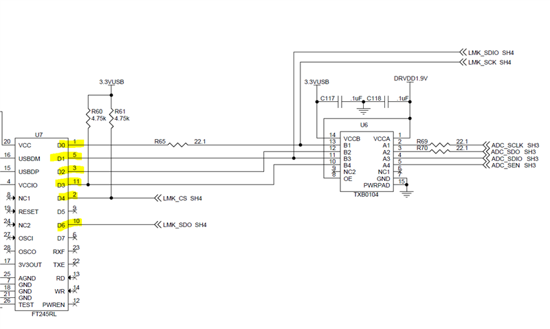
    This is easy to prototype using an external microcontroller (such as raspberry pi pico or arduino - just be sure to note that a 3.3V IO level is required for the LMK device SPI signals) by connecting GPIO to the following pins of the FT245RL device. Then in software, you can use already existing software packages to create a SPI interface for both the LMK and the ADC.


    All that is left is defining how you will "trigger" the SPI write sequence for the devices. You can do this by connecting another GPIO of the microcontroller to the test point labeled TP9. This is actually ideal as this is a testpoint for 3.3V and the microcontroller IO level should ideally be 3.3V to avoid having to up-translate using some external level shifter prior to connecting GPIO signals to the U7 chip above.

    In the microcontroller's main loop, check for if this IO (the GPIO connected to TP9) is high, and when high, enter a one-time block of code (using a flag) to write the desired configurations to the devices. This should achieve what you are looking to do using our hardware and a 3.3V logic microcontroller. (Note that most microcontrollers allow you to set the IO level using some VIO pin or similar)

    Thanks, Chase

  • Thank you. We may try this in the future. It would be helpful if you also provide a tool to translate LMK and ADC config files to SPI commands because it can be troublesome. In any case, we want to avoid using the Windows GUI.

    Thanks,
    Anastasios Xynos