This thread has been locked.

If you have a related question, please click the "Ask a related question" button in the top right corner. The newly created question will be automatically linked to this question.

ADS1119: RDATA not working

Part Number: ADS1119

Hello,

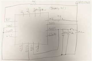
I'm breadboarding this ADC for a future design and having trouble getting readbacks from the device (I've made up two).  Here is a sketch of the circuit:

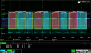
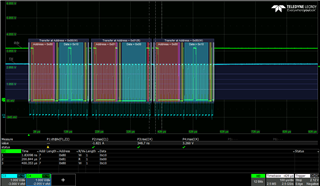
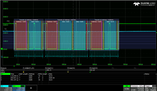
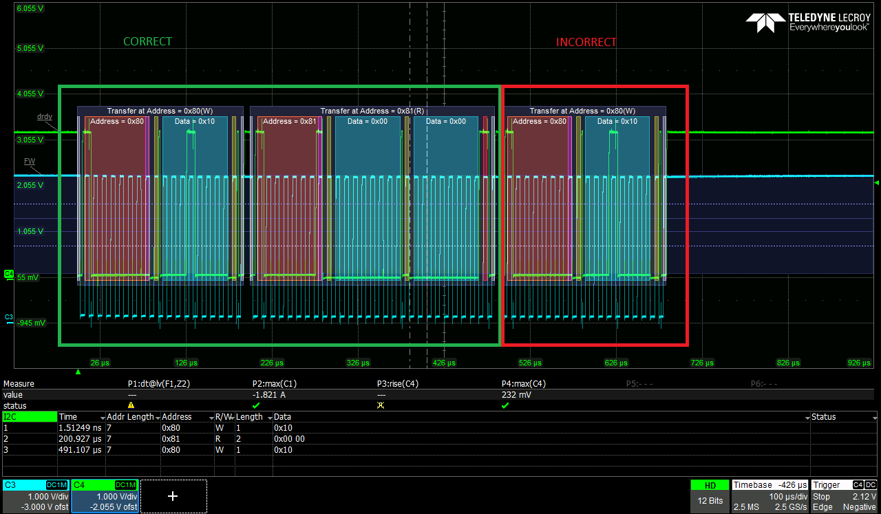
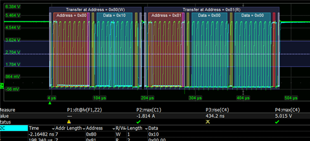
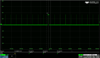
And a pic of DRDY as I try to read the back the ADC:

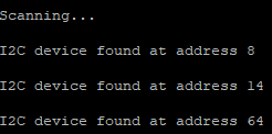
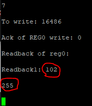
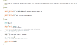
I'm sending the following commands (code, then terminal):

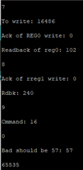
So power seems good, I2C is working, I can modify and read back registers, and DRDY shows both continuous readback as well as a longer interval when I'm reading back.  But the readback (I set the variable to a likely garbage number just to make sure the data is read back at all) is always FFFF.

I'm struggling with debug here - what are the best next steps to verify that things are working, and where I may have screwed up the implementation of likely the hardware?

Thanks in advance,

-Hugh Eisenman

  • I should note that these ADS1119s were sourced from Digikey.  I assume they're fairly safe as a distributor of genuine parts as long as I don't purchase through a 3rd-party seller.

  • Hi Hugh,

    Welcome to the E2E forum!  What I2C address are you using?  The drawing doesn't indicate what you are using (pins floating).  The best method for troubleshooting is to monitor the I2C bus.  You apparently are reading and writing ok, but what about the command you are using that differs (i2c_read_word as opposed to i2c_read_byte)?  What does the read_word function return?  Is it uint16_t?  Verify that you are getting the data as expected with the scope shots and that you are also receiving the proper ACK.  

    If read_word returns something other than uint16_t (uint32_t for example), you will eliminate the 16 bits of data and only get FFFF for the lower bits of data as the SCL continues to clock SDA which will now remain high after the conversion data are transferred.

    Best regards,

    Bob B

  • Hello,

    You are correct, A1/A0 are floating and I see address 64 (0x40) when I scan.

    read_byte and read_word are simple wrappers around the standard Wire library to reduce code complexity up front; this will be used by other developers later and I want to keep the main development efficient.  Code here:

    uint8_t i2c_read_byte(byte addr)
    {
      byte ack;
      Wire.requestFrom(addr, 1);
      ack = Wire.endTransmission();
      if (ack > 0) return(ack);
      delay(10);
      return(Wire.read());
    }
    uint16_t i2c_read_word(byte addr)
    {
      byte ack;
      uint16_t readback = 57;
      Serial.print("Bad should be 57: ");
      Serial.println(readback);
      Wire.requestFrom(addr, 1);
      ack = Wire.endTransmission();
      if (ack > 0) return(ack);
      delay(10);
      readback = Wire.read() << 8;
      readback |= Wire.read();
      return(readback);
    }

    Thank you for your prompt response,

    -Hugh

  • Hi Hugh,

    You cannot leave the address pins floating.  They must connect to something as these are digital CMOS input pins and there is no guarantee as to what value they will float to and how the ADS1119 will respond.

    • How do you distinguish a NACK from data? 
    • Did you verify your communication with the scope?  Or are you just relying on the results of your code? 
    • What SCL clock frequency are you using? 
    • What are the pullup resistor values on your I2C bus? 
    • What voltage are you applying to the inputs to compare your results?

    Best regards,

    Bob B

  • Hello,

    You're absolutely right, I appear to have one breadboard with address pins grounded, and one without.  Fixed.

    I'm relying on the existing I2C implementation within Arduino to deal with Ack/Nack, just checking that the return value of endTransmission(), which will return nonzero for NACK of any sort.  I'm also relying on Arduino for flow control; I believe the default frequency is 100KHz.  I'm using 1K pull-ups, sourced from the Teensy (my supply voltage for the ADC, in this case, is also the 3.3VREG bus from the Teensy).  Right now I have 0 and floating inputs attached to the ADC analog inputs; before I was using a DAC (to which I'm communicating fine) to generate a ~2.5V input.

    Here are some waveforms with decode.  Selection 7, set up the ADC for AIN0->GND, gain 1, 90sps, continuous sampling, internal reference:

    And here is the RDATA capture:

    I note that there is a nonzero readback in the 2nd byte that's read, but also that decode seems to show that the R/W bit in the 2nd byte is set to W, so perhaps I need to create a special readback for this ADC's response specifically.

    I appreciate your thoughts,

    -Hugh

  • I noticed a bit of a bug in my code; I was only requesting one byte back in read_word.

    When I fixed that I see the following capture:

    This appears to imply that a non-zero readback occurs sometime after my request and subsequent readback from the device occurs.  Very interesting.

  • Hi Hugh,

    Note that in both the register read (RREG) and the RDATA sequence there is an extraneous command that is sent at the end of the sequence.  I copied your data from the RDATA command and show below what is incorrect in the transmission sequence.

    This extraneous command may be a part of the issue you are seeing.  The data is showing as 0x0000, does your code report this value or are you seeing something different.

    Best regards,

    Bob B

  • Hi Bob,

    I agree it's puzzling.  Playing around with my code a bit adds to the confusion:

    This is the R/W of the following code:

           ADS1119_write_reg(ADS1119_ADDRESS, ADS1119_MUX_PCH0_NGND, ADS1119_GAIN_1, ADS1119_90SPS, ADS1119_CONTINUOUS, ADS1119_VREF_INT);

    Going to the function:

    void ADS1119_write_reg(byte addr, uint8_t mux,uint8_t adc_gain,uint8_t data_rate,uint8_t conversion,uint8_t vref)
    {
      uint8_t to_write = 0x0, rdbk = 0x0;
      uint16_t payload = 0x0;
      
      byte ack = 7;
      to_write |= mux;
      to_write |= adc_gain;
      to_write |= data_rate;
      to_write |= conversion;
      to_write |= vref;
      
      payload = ADS1119_WREG << 8;
      payload |= to_write;
      
      Serial.print("To write: ");
      Serial.println(payload);
    
      Serial.print("Ack of REG0 write: ");
        
      Serial.println(i2c_write_word(ADS1119_ADDRESS, payload));
    
      i2c_write_byte(ADS1119_ADDRESS, ADS1119_RREG0);
      Serial.println("Readback of reg0: ");
      Serial.println(i2c_read_byte(ADS1119_ADDRESS));
      return;
    }

    And to make sure that extraneous information wasn't getting put onto the bus I modified the read_byte code:

    uint8_t i2c_read_byte(byte addr)
    {
      byte ack;
      Wire.requestFrom(addr, 1);
      ack = Wire.endTransmission();
      if (ack > 0) return(ack);
      delay(10);
      Serial.print("Readback1: ");
      Serial.println(Wire.read());
      return(Wire.read());
    }

    The first byte attempted to be read off the line is printed within read_byte and the 2nd byte (because if my uC made a second read request we should see another byte posted by the ADC) is returned at the end.  The readback I see is:

    102 is correct (0x66 was sent in, 0x66 is read back) and 255 implies (as shown in the waveform above) that no additional valid bits were read from the bus.

    I don't know why I'm seeing that ghost on the scope; obviously it's THERE, but the ADC doesn't seem to be reacting to it and my uC can't seem to get any data from its issuance.

    Regards,

    -Hugh

  • Hi Hugh,

    I don't see anything obvious here either, but you can't discount that there could be a potential issue.  Did you verify with the scope the order of events in this last experiment?  I am guessing that as the data you are seeing is 0xFF, that the last command is not sent until after you send the second Wire.read.

    Now back to the original issue of the RDATA command, is this now working as expected?

    Best regards,

    Bob B

  • Hello,

    For debug purposes I've made a couple of changes to the setup and created some A-B comparisons.  I also have an ADI DAC (previously unpowered) on the line which is known working and can use that code/device to validate I2C.  Changes are:

    • ADS1119 and AD5667BRMZ are now on a 5Vdd
    • Teensy I2C, on 3.3V TTL, is going through a level-shifter to talk to the rest of the bus.  This was previously tested working and, as you'll see, still working fine.
    • I had previously not had helper functions read_byte/read_word/write_byte/write_word when I was developing the 5667 communication.  I have now tried using both write_byte and expanded code on the 5667.

    Example code:

        case 0:
            ack = i2c_write_byte(AD5667_ADDRESS, AD5667_CMD_REF_SETUP + AD5667_REG_DAC_A);
    /*        Wire.beginTransmission(AD5667_ADDRESS);
            Wire.write(AD5667_CMD_REF_SETUP + AD5667_REG_DAC_A);
            Wire.write(1);
            ack = Wire.endTransmission();
    */        sprintf(buf,"Response: %d",ack);
            Serial.println(buf);
            Wire.beginTransmission(AD5667_ADDRESS);
            Wire.write(AD5667_CMD_REF_SETUP + AD5667_REG_DAC_B);
            Wire.write(1);
            ack = Wire.endTransmission();
            sprintf(buf,"Response: %d",ack);
            Serial.println(buf);
            break;

    DAC A is enabled with write_byte, DAC B with the expanded code (which is basically still just write_byte).  I2C waveform capture:

    So...functions are working, and that ghost doesn't seem to happen with the AD5667.

    I will go back and try some A-B comparisons with expanded code vs. functions on the ADS1119 in the next few hours, posting my results here.

    Regards,

    -Hugh

    PS I had 1V asserted on AIN0, with internal reference selected, so I believe I should have been seeing ~40% full-scale (26214 or thereabouts).  I saw 0.  So not fixed yet.

  • Hi Hugh,

    Keep in mind that with the DAC you are just sending writes to the device.  With the ADS1119 you send a write command which seems to work fine, but following the read you see the write command that shows a second time.  The second write command to the device occurs sometime after the read is executed.  This would imply that you have another write command somewhere in your loop that is executing with the previous command contents.

    Best regards,

    Bob B

  • Hi Bob,

    You were right, I made a silly mistake I haven't thought about in a long time.  Arduino doesn't require an endTransmission after a requestFrom; that caused the extraneous re-issue of the previous write command (which apparently is still in the buffer from the last time something was written).

    Updated code:

    uint16_t i2c_read_word(byte addr)
    {
      byte ack, hbyte = 0, lbyte = 0;
      uint16_t readback = 57;
      Wire.requestFrom(addr, 2);
      //ack = Wire.endTransmission();
      //if (ack > 0) return(ack);
      delay(10);
      Serial.print("Available: ");
      Serial.println(Wire.available());
      hbyte = Wire.read();
      lbyte = Wire.read();
      Serial.println(hbyte);
      Serial.println(lbyte);
      readback = hbyte << 8;
      readback |= lbyte;
      return(readback);
    }

    New scope shot:

    And still the wrong readback.

    At this point I'm fairly confident I am communicating correctly with the IC; this feels more like a hardware issue than a software issue, even if my software continues to need improvement and refinement.

    I believe that I have AVDD higher than DVDD, REFP attached to AVDD, etc.  Is there a known condition of the ADS1119 which would consistently elicit, from a powered communicating ADC, consistent 0 or consistent FFFF?

    Thanks in advance.

    -Hugh

  • Hi Hugh,

    It appears that you have the RDATA command working as it should, but did you also fix the similar issue when reading the register data?  I would suggest that you verify the RREG command is also working properly and there is no repeated command write following the data.

    In some of the early scope shots you showed DRDY as toggling.  Is this still the case?  Once you have configured the ADS1119 for continuous conversion mode you need to issue the START/SYNC command.  Are you doing this?  The ADS1119 defaults to single-shot mode.  When setting the register to continuous mode you need to issue the START/SYNC command to start conversions.  If this is not done, then the RDATA command will only return what is in the internal conversion result buffer and will not show valid conversion data.

    Another possible issue might be related to power.  If there is a voltage sag (perhaps a bad supply/ground connection) when the ADC starts to convert and draws more power it is possible that the ADC has reset to the default conditions.  If you read the register following the START/SYNC command then if you see the default values instead of the previously programmed values then most likely there was a device reset.  A device reset could also occur from ESD or overvoltage on the input.  These are just some of the possible hardware issues you may encounter with a prototype using a breadboard.

    Best regards,

    Bob B

  • Success!  Let me address each of your points, however.

    I had previously checked readback of RREG0 and RREG1; they were both working, and the I2C looked correct, no extraneous writes at the end.

    The problem was START; I didn't do it.  Now that I have IC functions working I'll be creating better functions to control all of the aspects of the IC, lumped.

    The last oddity I'm seeing (and not a big issue at all) is that VREF_INT appears to be reading back voltages correctly, VREF_EXT (REFP tied to AVDD, REFN tied to common GND) reads AIN0/2.

    I will characterize more across the entire ADC range to validate linearity etc. but I think this did it.  Thank you, very much, for patiently working me through my silly mistakes.

    -Hugh

  • Hi Hugh,

    Glad to hear you've made progress.  As to the values you are reading back when using the external reference, keep in mind that you need to adjust the code value to the AVDD supply voltage in your calculation.  The internal reference is 2.048V and when applying a 1V input voltage you will get approximately 1/2 of full-scale, but the full-scale range changes with a larger reference voltage.  This results in a much lower returned code as now your full-scale range increases resulting in the value of one code having a larger value.

    LSB (or the value for a single code) = +/- VREF / (2^16 - 1) = 2* VREF / 65535

    Which is 62.5uV for 2.048V reference and 152.6uV for a 5V reference.

    Best regards,

    Bob B

  • Hi Bob,

    Characterization values pasted below:

    DAC V ADC RBK INT ADC V V-V0 ADC RBK EXT ADC V V-V0
    0.0015 12 0.000916 5 0.000763
    0.1 1614 0.12314 0.122225 662 0.101013 0.10025
    0.2 3213 0.245136 0.121996 1317 0.200958 0.099945
    0.3 4811 0.367056 0.12192 1972 0.300903 0.099945
    0.4 6406 0.488746 0.121691 2626 0.400696 0.099792
    0.5 8002 0.610513 0.121767 3281 0.500641 0.099945
    0.6 9599 0.732357 0.121843 3935 0.600433 0.099792
    0.7 11194 0.854047 0.121691 4589 0.700226 0.099792
    0.8 12790 0.975814 0.121767 5243 0.800018 0.099792
    0.9 14388 1.097734 0.12192 5899 0.900116 0.100098
    1 15988 1.219806 0.122072 6555 1.000214 0.100098
    1.1 17584 1.341573 0.121767 7209 1.100006 0.099792
    1.2 19182 1.463493 0.12192 7864 1.199951 0.099945
    1.3 20781 1.585489 0.121996 8520 1.300049 0.100098
    1.4 22379 1.707408 0.12192 9175 1.399994 0.099945
    1.5 23977 1.829328 0.12192 9830 1.499939 0.099945
    1.6 25574 1.951171 0.121843 10485 1.599884 0.099945
    1.7 27173 2.073167 0.121996 11140 1.699829 0.099945
    1.8 28770 2.19501 0.121843 11795 1.799774 0.099945
    1.9 30367 2.316854 0.121843 12450 1.899719 0.099945
    2 31964 2.438697 0.121843 13105 1.999664 0.099945
    2.1 32767 2.499962 0.061265 13759 2.099457 0.099792
    2.2 14414 2.199402 0.099945
    2.3 15069 2.299347 0.099945
    2.4 15724 2.399292 0.099945
    2.5 16379 2.499237 0.099945
    2.6 17033 2.59903 0.099792
    2.7 17687 2.698822 0.099792
    2.8 18343 2.79892 0.100098
    2.9 18998 2.898865 0.099945
    3 19673 3.001862 0.102997
    3.1 20327 3.101654 0.099792
    3.2 20982 3.201599 0.099945
    3.3 21644 3.302612 0.101013
    3.4 22299 3.402557 0.099945
    3.5 22953 3.50235 0.099792
    3.6 23608 3.602295 0.099945
    3.7 24264 3.702393 0.100098
    3.8 24919 3.802338 0.099945
    3.9 25580 3.903198 0.100861
    4 26235 4.003143 0.099945
    4.1 26891 4.103241 0.100098
    4.2 27546 4.203186 0.099945
    4.3 28200 4.302979 0.099792
    4.4 28855 4.402924 0.099945
    4.5 29509 4.502716 0.099792
    4.6 30164 4.602661 0.099945
    4.7 30825 4.703522 0.100861
    4.8 31480 4.803467 0.099945
    4.9 32134 4.903259 0.099792

    My DAC has ~3mV offset which I compensated at 3.0V, accounting for the slight jump in values.  The internal reference at 2.048 gives a slightly problematic scaling factor when applied to a 5V (4.096 of course would be perfect).  But the external reference appears to be working perfectly and will be just fine for the bused supply voltage I'll be using for...well, quite a few of these.  The linearity, by the way, is VERY good for my admittedly not-particularly-granular application.

    Thank you again for all of your help, I can now go CAD up a board.