This thread has been locked.

If you have a related question, please click the "Ask a related question" button in the top right corner. The newly created question will be automatically linked to this question.

ADC3660: Waking the spi registers up.

Part Number: ADC3660

So here we go, manual operation of the ADC3660.

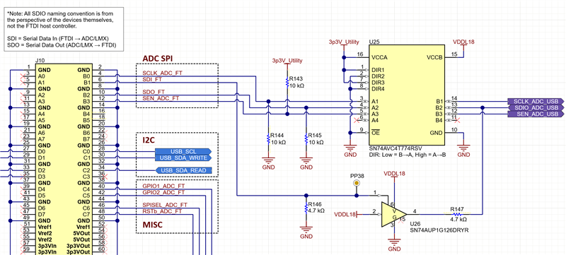
So the tristate buffer enable is on a gpio pin.

I wiggle the bits as prescribed in the data sheet and nothing.

Can't tell if I have a successful write and I can see the read was unsuccessful.

So what are the minimal software steps for getting the ADC3660s spi registers turned on?

p.s. What was the benefit of using 3-wire spi on the ADC3660? With 8 no connect pins on the part, you certainly had room. Now with zero support, you didn't do anyone any favors. 

  • Thomas,

    The serial interface is active by default without any steps. Which buffer are you referring to? Do you have access to measure power consumption on supply rails? If so, what I personally do while debugging initial SPI issues is see if writing to powerdown decreases power consumption. If you do not have access to supply current, what you can do is write to DCLK OB EN to disable to DCLK output buffer. You should be able to measure this on a scope and see the DCLK output disappear if the SPI write is successful.

    I understand the frustration of lacking 4w SPI. I prefer 4w SPI myself also. But this device is a part of a larger device family which utilizes the same package and the no connect pins from this specific device variant are implemented on other variants. Most customers are leaning towards 3w SPI due to lower I/O count dedicated to the device by costly FPGA so the designers are leaning towards a 3w SPI interface for all devices moving forward. To use a 4w SPI interface, a tri-state buffer can be implemented on the SDIO line to use 4w SPI controller as shown in the example below. 

    Regards, Chase