This thread has been locked.

If you have a related question, please click the "Ask a related question" button in the top right corner. The newly created question will be automatically linked to this question.

ADS124S06: ADS124S06: Frist ADC Data output is not correct for Multi slave SPI connections, Other two ADCs data output is correct in Same SPI.

Part Number: ADS124S06
Other Parts Discussed in Thread: TMS570LS3137, , ADS124S08

Dear TI team, 

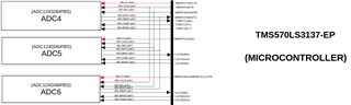
We are using ADS124S06 device for one of the differential measurement, I have connected three ADCs in single SPI of  TMS570LS3137.

Below image refers my Digital interface with controller (NHET and CAN pins are using as a GPIO). Wherever we read rata from ADC4 its always getting wrong values like for 5mV its reading as 9mV, for 100mV its 156mV, for 500mV is 625mV and for 1000mV its 1250mV. (My gain setting is default as 1)

We are using same DIN and Just switching CS pin alone to read ADC5 and ADC 6 we are able to get correct data’s like  for 10mV its 10mV, for 100mV its 100mV and for 1000mV its 1000mV. For calculations we are using same single loop for all Data buffers.   

We are using two SPIs (MibSPI1 and MibSPI3) distributed 3 ADCs for each. We have seen same behaviour in Both the SPI chains. Also we have checked with different boards also but the issue is similar between boards.  

For hardware wise there is a No difference between All 6 ADCs.. All are similar as recommended in ADS124S08/06 EVM board.    

Please kindly do the needful to resolve the above issue.

Thanks and regards,

Venugopal B.

  • Hi Venugopal B.,

    If you have two sets of SPI device chains, and both chains are acting the same way you should review your code and timing related to the conversion and response of your system.  It would be helpful to know all the device configuration settings you are using and how you are controlling the start of conversion.  Also, how are you determining when the conversion has completed and is valid?

    Besides the communication and timing of capturing the conversion, in the analog domain the conversion requires a valid and settled reference input.  If the reference hasn't settled then you will see what appears to be a gain error.  So analog settling of your system could also exhibit this kind of behavior.  

    So I would suggest reviewing the timing of your system response relative to the events just prior to reading the conversion data of the first ADC in the loop.  For example, if you are using the internal reference and powering it down between loops, then you need to make sure that you wait a significant amount of time for the reference to settle before starting the conversion.

    If you have access to a logic analyzer, it would be useful in troubleshooting to help identify differences in process flow of the software.

    Best regards,

    Bob B

  •  Hi Sir, 

    Thank you for your response. 

    We get resolved the issue, the problem we found that due to some issue Chip select Pin mux of ADC 3 is always low when we read ADC1 data.. So some junk Value is mixing up with ADC1 Data.

    Instead of CS mode we configured Pin MUX as GPIO and issue get resolved. Chip select Mode is not working properly for Both the SPIs. 

    Thanks and regards,

    Venugopal B