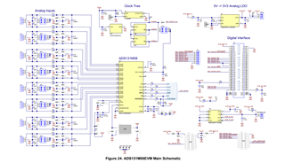
Other Parts Discussed in Thread: , ADS131M04
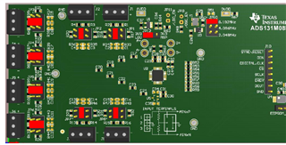
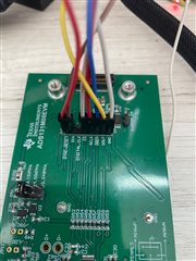
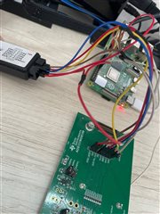
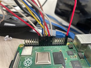
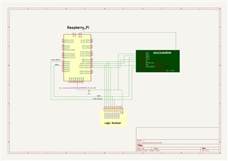
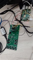
Hello, some time ago I purchased an ADS131M08EVM to conduct tests, but now I need to step out of my comfort zone and start implementing it with the board using a Raspberry Pi 4b. I want to use a Raspberry Pi 4b to control the ADS131M08 via SPI by programming in the Python language. My goal is to start by reading the registers, using the default values provided in the datasheet as a foundation.
I'm not sure if my code is well structured
CODE:
import spidev
import RPi.GPIO as GPIO
import time
class ads131m08():
# ADS131M08 commands
commands = {
'CMD_NULL': [0b00000000, 0b00000000], # Request ads samples
'CMD_RESET_DEVICE': [0b00000000, 0b00010001], # Reset the device
'CMD_STANDBY': [0b00000000, 0b00100010],
'CMD_WAKEUP': [0b00000000, 0b00110011],
'CMD_LOCK': [0b00000000, 0b10101010],
'CMD_UNLOCK': [0b00000000, 0b11001010],
'CMD_RREG': [0b10100000, 0b00000000], # Read register
'CMD_WREG': [0b01100000, 0b00000000], # Write register
}
def __init__(self, SyncResetGpio, DrdyGpio, DeviseSpi, cs, sclk=12000000):
# SPI configuration
self.spi = spidev.SpiDev()
self.spi.open(DeviseSpi, cs)
self.spi.max_speed_hz = sclk
self.spi.mode = 1
self.spi.lsbfirst = False # default
# ADS131M08 operates in mode 1
self.ChEnable = 8
# GPIO configuration
GPIO.setwarnings(False)
GPIO.setmode(GPIO.BCM)
GPIO.setup(DrdyGpio, GPIO.IN) # To read the pin --> DrdyState = GPIO.input(DrdyGpio)
GPIO.setup(SyncResetGpio, GPIO.OUT) # To write the pin HIGH = Deactivate, LOW = Activate --> GPIO.output(SyncResetGpio, GPIO.LOW)
# GPIO.output(SyncResetGpio, GPIO.HIGH)
GPIO.setup(self.ChEnable, GPIO.OUT)
GPIO.output(SyncResetGpio, GPIO.LOW)
time.sleep(1)
GPIO.output(SyncResetGpio, GPIO.HIGH)
def id(self):
GPIO.output(self.ChEnable, GPIO.LOW)
respons = self.spi.xfer2([0xA0, 0x01, 0x00]) # Sending the read command with address 0x01 (status)
GPIO.output(self.ChEnable, GPIO.HIGH)
print("STATUS: ", respons)
time.sleep(1)
def close(self):
self.spi.close()
def invert(self):
print("Inverts the bits to use mode 3 as mode 1")
ads = ads131m08(22, 24, 0, 0, 1000000)
try:
while True:
ads.id()
except KeyboardInterrupt:
ads.close()
GPIO.cleanup()
RESULTS:
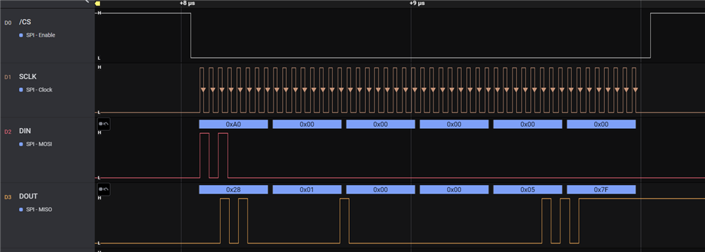
STATUS: [255, 40, 0]
STATUS: [224, 1, 0]
STATUS: [5, 255, 0]
STATUS: [224, 1, 0]
STATUS: [5, 255, 0]
STATUS: [224, 1, 0]
STATUS: [5, 255, 0]
STATUS: [224, 1, 0]
STATUS: [5, 255, 0]
STATUS: [224, 1, 0]
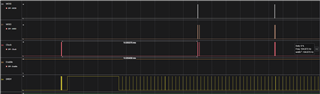
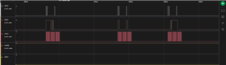
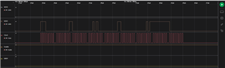
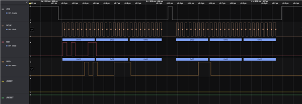
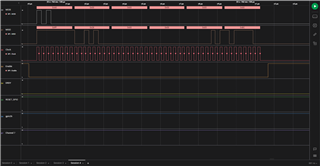
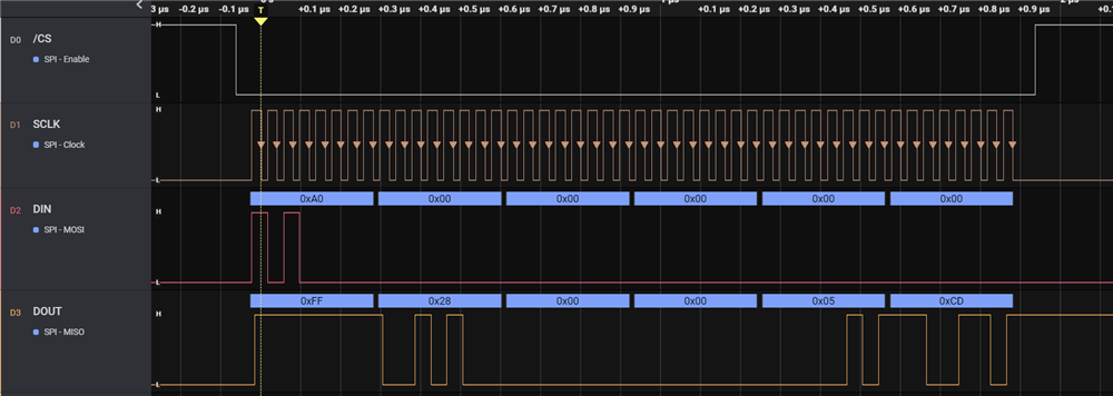
For the same command, I'm receiving various responses and none are as expected --> 0x0500h.
For --> respons = self.spi.xfer2([0xA0, 0x00, 0x00])
RESULTS: STATUS: [255, 40, 0]
STATUS: [40, 1, 0]
STATUS: [40, 1, 0]
STATUS: [40, 1, 0]
STATUS: [40, 1, 0]
STATUS: [40, 1, 0]
STATUS: [40, 1, 0]
STATUS: [40, 1, 0]
STATUS: [40, 1, 0]
STATUS: [40, 1, 0]
For the same command, I'm receiving various responses and none are as expected ID --> 0x28XXh.
For --> respons = self.spi.xfer2([0xA0, 0x03, 0x00])
RESULTS:
STATUS: [255, 40, 0]
STATUS: [224, 3, 0]
STATUS: [5, 255, 0]
STATUS: [224, 3, 0]
STATUS: [5, 255, 0]
STATUS: [224, 3, 0]
STATUS: [5, 255, 0]
STATUS: [224, 3, 0]
STATUS: [5, 255, 0]
For the same command, I'm receiving various responses and none are as expected --> 0xFF0Eh.