This thread has been locked.

If you have a related question, please click the "Ask a related question" button in the top right corner. The newly created question will be automatically linked to this question.

DAC39RF10EVM: some questions

Part Number: DAC39RF10EVM
Other Parts Discussed in Thread: TPSM82913

Hi team,

There are some questions in order to undestand the EVM schematic and use the schematic as reference for the designing.

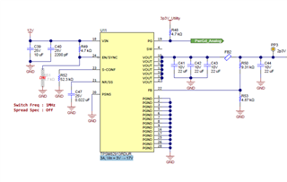
Q1. Could you tell the meaning of "3A, Vin = 3V → 17V" in the figure below?
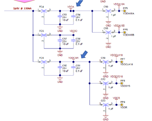
Q2. It seems that VDDA and VDDCSR exist in only the figure below in the schematic P.7. Are there any purpose to use VDDA and VDDCSR here? 
Q3. In the P.17 of the schematic, we can see the schematic as bleow. Could you tell the PCB pattern of the shcematic?

Regards,

Noriyuki Takahashi

  • Hi Noriyuki,

    Please find comments below.

    Q1. Could you tell the meaning of "3A, Vin = 3V → 17V" in the figure below?

    This comes from our internal parts library indicating that this TPSM82913 is a device capable of a 3V to 17V input range and a 3 amp output capacity.

    Q2. It seems that VDDA and VDDCSR exist in only the figure below in the schematic P.7. Are there any purpose to use VDDA and VDDCSR here? 

    These are just net labels, not test points. These are used to make routing easier. If these are not used, when routing the PCB, a name such as NetC60_2 would show. Instead of wondering what this NetC60_2 is referring to, we can easily tell that this would be VDDCSR (our internal name to represent the shared rail which is distributing to VDDCLK18, VDDSYS18, and VDDR.

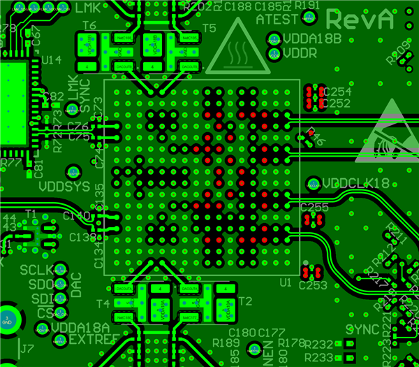
    Q3. In the P.17 of the schematic, we can see the schematic as bleow. Could you tell the PCB pattern of the shcematic?

    I am assuming you are asking about the layout for these local decoupling capacitors? If this assumption is incorrect, my apologies, but I would ask you to please re-phrase the question for me.

    These act as local de-coupling for each of the areas of the device where DVDD is required. 

    Regards, Chase