


Other Parts Discussed in Thread: ADC12DJ5200RFEVM, TPS7H1101A-SP
We are trying to figure out the limitations with separating VD11 and VA11, if any. Initially we were planning on matching the power tree shown in Figure 8-3 of the datasheet, which supplies both rails from a common LDO.
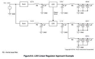
We ran into an issue where the combined max current from VD11 and VA11 exceeds the 3A max output current of the TPS7H1101A-SP, when accounting for EEE-INST-002 derating of 80%. For this reason we determined our safest course of action would be to separate them to two regulators. It seems the ADC12DJ5200RFEVM powers VA11 from different regulators (one a buck and one an LDO), so this approach has merit. One caveat: the below note from the datasheet implies there can be issues when VD11 and VA11 are not sequenced correctly and/or don't track.
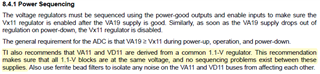
Can you please clarify what issues we need to look out for when deriving VA11 and VD11 from different regulators? Our preferred solution would be to use 2x TPS7H1101A-SP sharing an enable input. Is there a max permissible deviation we need to maintain in normal operation & during power-on?
