This thread has been locked.

If you have a related question, please click the "Ask a related question" button in the top right corner. The newly created question will be automatically linked to this question.

ADS5560: Data converters forum

Part Number: ADS5560
Other Parts Discussed in Thread: LMH6552, THS4509, ADS5500

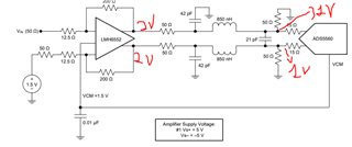
First of all, as far as I saw in the data sheet, I saw that the ads5560 works with external 1.5V. However, I could not find the 1.5V reference IC anywhere. Secondly, In page 46, why is 1.5V recommended at the minus terminal of the LMH6552? Is it recommended for 5V input stage? What is the effect on the noise of the signal if we do not use this 1.5V? Thirdly, Is the cut-off frequency of the anti-aliasing filter on page 46 20MHz? İs it true?

,

  • Hi Sefa,

    On the EVM schematic there is no 1.5V IC for the ADC common mode or the amplifier common mode because in that configuration the VCM for the ADC is generated internally and then the VCM pin of the ADC is outputting 1.5V that is then used as the input VCM for the amplifier. In general this is best practice as if you do not have this configuration you will have the common mode of the ADC and amplifier competing with each other which can lead to bad harmonic performance. Also in the ADC datasheet it says that VCM must be 1.5 +-0.01 V, if it is not this then the common mode for the ADC will be wrong and you will not get good performance.

    The diagram on page 46 shows 1.5V at the input of the amp to indicate this should be the common mode voltage for the amp. I am not sure if that particular amp has enough headroom to support a 5V input swing. 

    No the filter does not have a cutoff of 20MHz, it is 40Mhz. It is designed to align with the end of the first Nyquist zone at the ADCs max fs which is 80MHz.

    Best,

    Eric 

  • Hi Eric,

    1) I know that Vcm pin should given to amplifier. Thx for your reply

    2) In page 46 1.5V is recomended at minus terminal of LMH6552 and it is not same voltage with reference. Not CM pin. Why is it recommended?

    3)I also see that in page 46 behind of LMH6552 there are 50 ohm series resistor and 50 ohm paralel to series 15 ohm ? . If ı use this configuration . While I am driving 2 volt peak to peak sine wave. I am taking 1 volt peak to peak sine wave. Why is it recommended. 

  • Hi Sefa,

    1) I am not sure why there is a 1.5V at the minus terminal of the LMH6552, this seems out of place to me. One question for you do you wish to DC couple the amplifier to ADC or is AC coupling ok? If so you would want to add some AC coupling caps to the circuit.

    3) The 50 ohm parallels to ground are terminations for the two lines, the 15 ohm resistors are there to help limit kickback current from the adc when the internal sampling circuitry turns on and off. 

    Can you clarify this statement a bit "While I am driving 2 volt peak to peak sine wave. I am taking 1 volt peak to peak sine wave. Why is it recommended" Do you mean that you are inputting 2Vpp and outputting 1Vpp I am not exactly sure what you mean.

    Best,

    Eric

  • Hi Eric,

    1) I have analog input with 200kHz AC signal. 

    3) As you see in figure below, as ı understood, there is 50 ohm series and 50 ohm parallel termination. these termination resistors divide the voltage in half.

  • Hi Sefa,

    This is not correct, The 50ohms to ground serve as a shunt 100ohm differential termination.

    Unfortunately, the circuit in the datasheet and the amplifier circuit on the EVM do not match.

    Therefore the LMH amp/adc circuit probably has not been proven.

    If you can give us a few requirements for your application, we can help guide you on a similar design.

    Regards,

    Rob

  • Hi Rob I have buffered analog input single ended signal with 400mV amplitude and 200kHz frequency. I am looking for differential amplifier for ADS5560 to read signal with ADC’s full scale range.Input range of Adc can be adjusted with 3.56V or 3V.
    ı am also worried abour LVDS interface of ADC . Should I add termination resistor for FPGA connection.Thanks for your help.

  • I will arrange samplinf rate of ADC I am not sure yet. But at least 20 Msps. Thanks for your help in advance

  • Hi Sefa,

    Should I add termination resistor for FPGA connection.

    Yes, a physical termination resistor is always preferred over internal termination resistors. If your FPGA has the option to be terminated internally, be sure to disable this to avoid reduction of 2 of the termination resistance at receiver.

    I am moving this thread to our amplifier group for assistance in choosing differential amplifier.

    Regards, Chase

  • Hello Sefa,

    From the amplifier team: What supply voltages are available to use with the fully-differential-amplifier?  For example, the LMH6552 operates best on +/- 5V supplies and with AC-coupled inputs to avoid input common mode limitations.

    Regarding the 1.5V DC signal shown on Figure 60 of the ADS5560 Datasheet, I would recommend using other design guides and walk-throughs for selecting your amplifier and designing your circuit.  It is possible there was a case where having a DC voltage on the amplifier pin helped avoid violation of differential input voltage limits, but I do not think your application would encounter that issue.  In the reference material I point to below, all figures showcase the amplifier pin being connected to GND through passive components, no DC bias voltage present.  There is a common-mode voltage being set by the ADC at the amplifier's VCM pin.

    Within Section 8 of the LMH6552 datasheet there is information on how to setup the amplifier and drive an ADC.  The higher available supply voltage on the LMH6652 may be important to your application.  However, if you choose to AC couple the inputs of the amplifier to the FPGA/signal source you may not need the LMH6552; the THS4509 is used in other circuitry with ADS5560.

    On the ADS5560's available EVMs (& user guides) the selected amplifier is the THS4509, which has a Section 9 describing how to interface with ADS5500 family ADCs.

    Your signal voltage level and operating frequency should not be limited by either the THS4509 or the LMH6552.

    Please let me know if you are finding it difficult to select an amplifier or setup the ADC drive circuitry.

    I would advise you to check-in and ask questions whenever you encounter ambiguity or tricky topics, as you did with this thread.  As Rob mentioned, it is unlikely Figure 60 was explicitly tested exactly how it appears in the document.  A good practice is to check device EVMs to see how TI has designed the boards to evaluate the ICs. 

    Best,

    Alec