- Ask a related questionWhat is a related question?A related question is a question created from another question. When the related question is created, it will be automatically linked to the original question.
Hi, Support
Have couple question regarding the DAC37j84 datasheet, can you please help with it??
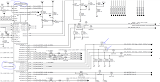
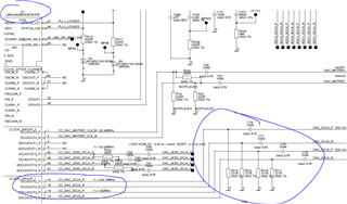
1. The DACCLKP/N and SYSREFP/N internal termination. from the datasheet, it shows 100 Ohm internal termination. Is this default hw 100 ohm there or need to config it?? I don't see it in the register map to config it.
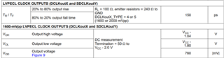
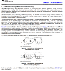
The reason for the ask is that when I sent PLL clock chip as LVPECL1600, the input differential voltage measured at the DACCLKP/N is about 1.7V. when set as LVPECL1600, it suppose to be about 800mV instead.
can you please help understand why? is it possible the termination is no on??
2. The analog output. The output compliance range is max 0.6V. This mean that if I config the full scale current output is 20mA and the output load resistor should be 25 Ohm. But if I place a higher value resistor, will it cause any damage of the chip or the output will just clamp to the max 0.6V??
thank you.
Li