Other Parts Discussed in Thread: LMK04828, LMK00304,
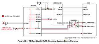
I see in the user manual there are four possible options for clocking the ADC and FPGA together. I'm looking into option 1 "EXT CLK from LMK to ADC" (Default). It looks like this configuration utilizes a reference clock to J31, and the LMK04828 produces the necessary clocks for the system. My question is why is the FPGA clock buffered and split by the LMK00304 into FPGA_GBT_CLK[0] and FPGA_GBT_CLK[1] prior to hitting the FPGA. Why not have the LMK04828 produce both of these clocks by using another one of the 14 possible clock outputs? It looks like all the FPGA clocks aside from FPGA_CLK are buffered using this LMK00304 device for all four clocking configurations. Are there any negative aspects to using this LMK00304 device to fan out the clocks for the FPGA?