This thread has been locked.

If you have a related question, please click the "Ask a related question" button in the top right corner. The newly created question will be automatically linked to this question.

Clarification on DAC8750 DAC part

Other Parts Discussed in Thread: DAC8750, DAC8760, SN6507, ISOW7741

Hi,

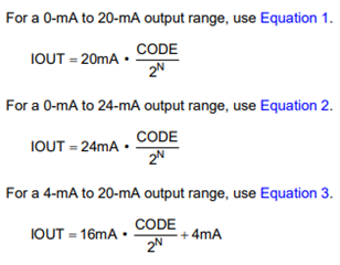
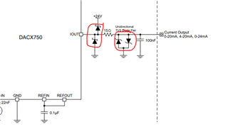
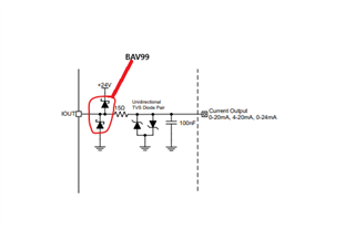
Currently I have selected DAC8750 DAC part for 4-20mA Application. Since I'm using DAC very first time in the design, i have following couple of query to be clarified.

  • What is the sampling rate of DAC8750 DAC ? since these detail is not mentioned in the datasheet. 
  • Can i use this DAC for 3 or 4 wire application? if so please share the reference design (3 and 4 wire) for the same.

Regards,

Chitharanjan M

  • Hi Chitharanjan,

    The sample rate of the DAC8750 is available on the product page and is 0.04 Msps.

    The DAC8750 can also be used as a 3 wire transmitter application. I don't think there's a specific design that uses the DAC8750, but a lot of designs use the DAC8760 (which is both voltage and current output).

    This video is very useful and shows both the DAC8760 and DAC8750. The DAC8760 3 wire design it mentions is TIPD199. I would recommend using these resources and removing any circuitry for the voltage out and sense pins since the DAC8750 doesn't include these.

    Let me know if you have any other questions!

    Thanks,
    Lucas

  • The sample rate of the DAC8750 is available on the product page and is 0.04 Msps.

    Thanks for detail....

    Similar DAC8760/50 , TI have any other DAC IC which is supporting higher sampling rate ? Because our main requirement is to DAC should support 4-20mA current out with >20MSPS

    Regards,

    Chitharanjan M

  • Hi,

    I don't think we have any other DACs that support a 4-20 mA output with a sample rate that high.

    The highest sample rate our buffered current output DACs support is 0.25 MSPS, but they don't have a built-in 4 - 20 mA range.

    I'd recommend checking out our product comparisons where you can filter the parameters of the DACs to your specifications:
    www.ti.com/.../overview.html

    Thanks,
    Lucas

  • HI Licas,

    Thanks for the details....

    We need to Galvanically isolate the DAC8670 circuit in digital and power side. Can you please suggest the below two parts?

    • Suggest the right part for isolating the SPI interface in DAC8750?
    • Also please suggest the suitable part for 24V power isolation. Currently in our design we have on board 24V power just we need to isolate and give to DAC AVDD pin.

    Regards,

    Chitharanjan M

  • Hi Chitharanjan,

    I've had a good experience using the ISO6741 and ISO7641 with another high precision DAC to isolate SPI signals.

    Are you looking to provide the DAC8750 with 24 V or a lower voltage? This document recommends the SN6507 which converts it down 15 V.

    Let me know if these work for you,

    Thanks,
    Lucas

  • Are you looking to provide the DAC8750 with 24 V or a lower voltage? This document recommends the SN6507 which converts it down 15 V.

    I'm planning to give 24V to DAC AVDD pin and Looks SN6507 also supports 24V-->24V if we choose 1.09 transformer as shown in below table. Can you please confirm on this? can I use SN6507 for 24V application? 

    Or do you have any integrated isolated DC-DC converter with integrated transformer for this application?


    Regards,

    Chitharanjan M

  • Also Do you have any single supply isolator for SPI interface? 

    Regards,

    Chitharanjan M

  • Hi Chitharanjan,

    Lucas is not in office today, he will review your question after the weekend. 

    Best,
    Katlynne Jones 

  • Hi Chitharanjan,

    Yes, you can use the SN6507 for the 24V -> 24V application with the respective transformer.
    A lot of the integrated transformer parts have dual outputs or are intended for driving gates, like the UCC15240.

    If you are looking for a SPI isolator with integrated power isolation, the ISOW7741 may fit your needs.

    Let me know if you have any other questions,

    Thanks,
    Lucas


  • HI Burnette,

    If you are looking for a SPI isolator with integrated power isolation, the ISOW7741 may fit your needs.

    I have below query, can you please clarify?

    Can I use below circuit in my design? Here I'm going to feed VIO=1.8V and VSEL=GND which means VISOOUT is selected as 3.3V power supply. Because in two side of the isolator working with two different voltage potential. Is this recommended? 

    I have selected VIO=1.8V since FPGA IOs are 1.8V voltage level.

    Regards,

    Chitharanjan M

  • Hi Chitharanjan,

    I believe for that part, in order to get 3.3 V out at the VISOOUT pin, you need to provide 5 V or 3.3 V for VDD, not 1.8 V.
    IOVDD could still be 1.8 V, but you would need a higher voltage for VDD.


    Thanks,
    Lucas

  • Hi Lucas,

    Thanks for the suggestion....

    Can you please let me know what type of front end circuit to be used for DAC8750? Is there any recommended filter circuit ? and What is the recommended support circuitry for 3 and 4 wire configuration?  If you have reference design where 3 and 4 wire configuration used, please share.

    Regards,

    Chitharanjan M

  • Hi Chitharanjan,

    The closest thing we have to a reference design is the TIPD119, which shows the DAC8760 as a 3-wire transmitter.
    If this design fits your needs, you should be able to remove any VOUT/Sense circuitry to minimize the design and support the DAC8750.

    Thanks,
    Lucas

  • HI Lucas,

    In DAC8750,

    1. Is it must to connect HART-IN pin to FSK modulation? or Can we connect it to ground through 22nF as  shown in reference design is the TIPD119.
    2. What is the termination method of ALARM and CLR pin if it not used?

    Regards,

    Chitharanjan M

  • Hi Chitharanjan,

    1. If you have no need for HART modulation in your design, you can connect the HART-IN pin to ground using the 22nF capacitor.

    2. Section 9.2.2 of the datasheet mentions that ALARM and CLR can be connected to GND if they will not be used. I do recommend having a pullup resistor of ALARM to DVDD in the event that debugging / error checking is needed.

    Thanks,
    Lucas

  • Hi Lucas,

    Thanks for the update.

    I would like to know how to verify the DAC8750 IOUT whether it can generated properly? Is there any test methodology?

    Is there any formula to convert the digital transmitted value to current and So that it can be compared with measured value?

    Kindly share the above details......

    Regards,

    Chitharanjan M

  • Hi Chitharanjan,

    Equations for the CODE to IOUT conversion can be found in the datasheet, if I understand your question.
    I would use the appropriate equation to calculate the expected IOUT and use a reasonable resistive load or multimeter to verify the DAC's performance.


    Since the DAC8750 is a 16-bit DAC, 2^N would be 65536 and your CODE would range from 0 - 65535.


    Thanks,
    Lucas

  • HI Lucas,

    Thanks for the detail.....

    May I know how to measure the IOUT current? Is there any specific device to be procured to measure the IOUT current? Or can we measure the IOUT current through 300E as mentioned in EVK?

    I believe for that part, in order to get 3.3 V out at the VISOOUT pin, you need to provide 5 V or 3.3 V for VDD, not 1.8 V.
    IOVDD could still be 1.8 V, but you would need a higher voltage for VDD.

    I still have query on above,

    • In my design I have connected VDD to 3.3V, VISOOUT and VISOIN tied together and VIO is 1.8V, With this is configuration I can use this ISOW7741 as isolator and Level Translator (3.3V to 1.8V)?
    • With the above configuration, Since I have feeding 1.8V to VIO so that 2,3,4,5,6,7 pin level would be 1.8V? Similarly, since I have connected VISOIN to VISOOUT (3.3V) Field side IO would be 3.3V? is this works?

    Regards,

    Chitharanjan M

  • Also Please let know the recommended diode part number?

    Regards,

    Chitharanjan M

  • Hi Chitharanjan,

    Measuring IOUT:
    I would just measure the current on a resistive load, the datasheet uses 300 ohms for most graphs and measurements.

    ISOW7741:
    Yes, the configuration you described qualifies the highlighted case that I posted previously, with VDD 3.3 V, VIO 1.8 V, and VISOOUT outputting 3.3 V and shorted to VISOIN. You would be supplying the 1.8 V to VIO and the other side's digital IO would be 3.3 V. Make sure the EN pin is high as well.

    Diodes:
    For the two diodes connected to the IOUT pin, I recommend using a single BAV99-7-F.
    The two unidirectional TVS diodes can be substituted with a single bipolar TVS diode, which I recommend the CDSOD323-T15SC or any similar diode.

    Thanks,
    Lucas

  • Hi Lucas,

    For the two diodes connected to the IOUT pin, I recommend using a single BAV99-7-F.
    The two unidirectional TVS diodes can be substituted with a single bipolar TVS diode, which I recommend the CDSOD323-T15SC or any similar diode.

    As per the DAC8750 datasheet the maximum IOUT voltage would be AVDD-2 i.e. 24V since AVDD pin is connected to 24V supply in my design. In this case whatever you suggested CDSOD323-T15SC diode part will it work? because this part has 15V Voltage - Reverse Standoff which is very less than working voltage i.e 22V. 

    I have selected CDSOD323-T24SC with the same series which is having 24V Reverse Standoff. Please confirm on this can I use this part instead of CDSOD323-T15SC?

    For the two diodes connected to the IOUT pin, I recommend using a single BAV99-7-F.

    Thanks for the suggestion. Please confirm below connection for BAV99

    Regards,

    Chitharanjan M

  • Hi Chitharanjan,

    Yes, I apologize, you should use the CDSOD323-T24SC over the 15 V part I suggested. I was looking at my output protection for ±10 V by mistake.

    You are correct with your image as well, the circled diodes could be replaced with the BAV99-7-F, and the TVS pair on the right could be replaced by the CDSOD323-T15SC.

    Thanks,
    Lucas