This thread has been locked.

If you have a related question, please click the "Ask a related question" button in the top right corner. The newly created question will be automatically linked to this question.

ADS131M06: Crosstalk between channels

Part Number: ADS131M06

Hello, 

I measured crosstalk of the ADS131M06.

Case 1: channel 0 in measurement range, channel 1 to 5 are clipping with measured values above 1.2V.

measured values with ADC

[[-0.21721458, 1.19999986, 1.19999986, 1.19999986, 1.19999986,1.19999986]] 

Case 2: all channels in measurement range.

[[-0.03692994, -1.05122795, 0.1748198 , -0.69474978, -0.89339933,-0.69500842]]

Value for channel 0 is 0.2V lower with all channels in measurement range. When I probe channel 0 with a scope I see that the voltage of S1 remains constant  independent of S2 - S6. What is going on here?

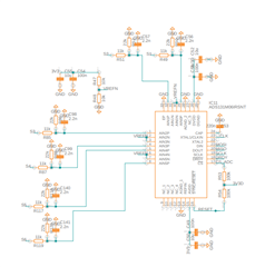
some more details and schematics.

Original signals S1, S2 until S6 range between 0 and 5V. 

These are reduced with a voltage divider to 0 - 3.3V range. 

When channels 1 to 5 are clipped this means that S1 to S5 are 5V. 

After the voltage divider this means 3.3V on the AINXP pins. On the AINXN pins there is +1.65V reference voltage.

Best regards, 
Christiaan

  • Hi Christiaan,

    In case 1, what's your voltage applied to VAINxP pin when you saw the measured value from the ADC is clipped to 1.2V? 

    In case 2, can you explain "I see that the voltage of S1 remains constant  independent of S2 - S6"? What's your input on S2-S6 and what did you see on S2-S6 or ADC's output?

    Thanks&regards,

    Dale

  • Hello Dale, 

    Thanks for your response. 

    In case 1 the value on the VAINxP pin is 3.3V when it is clipped to 1.2V. 

    See table below for the values of S1-S6. 

    In case 1 the values of s2-s6 are set to 5V. In Case 2 they are ranging from 0.7 to 2.6V.  The voltage on VAIN0P is identical for case 1 and case 2. Still the output of the ADC differs 0.2 V between case 1 and case 2. 

    case 1
    output ADC 1 output ADC 2 output ADC 3 output ADC 4 output ADC 5 output ADC 6
    -0.23 1.20 1.20 1.20 1.20 1.20
    AI0P AI1P AI2P AI3P AI4P AI5P
    1.57 3.40 3.40 3.40 3.40 3.40
    AI0N AI1N AI2N AI3N AI4N AI5N
    1.65 1.65 1.65 1.65 1.65 1.65
    S1 S2 S3 S4 S5 S6
    2.36 5.1 5.1 5.1 5.1 5.1
    case 2
    output ADC 1 output ADC 2 output ADC 3 output ADC 4 output ADC 5 output ADC 6
    -0.039 -1.084 0.128 -0.725 -0.923 -0.725
    AI0P AI1P AI2P AI3P AI4P AI5P
    1.57 0.49 1.76 0.88 0.65 0.87
    AI0N AI1N AI2N AI3N AI4N AI5N
    1.65 1.65 1.65 1.65 1.65 1.65
    S1 S2 S3 S4 S5 S6
    2.36 0.73 2.64 1.32 0.98 1.3
  • Hi Christiaan,

    In case 1:

    1. The 1.2V voltages you saw from the ADC output on all channels except the first channel (ADC 1) are correct because you input signal already exceeded the maximum input range of the ADC, the full-scale range of ADS131M06 ADC is +/Vref/Gain, your Gain=1 and the internal Vref is 1.2V, so the maximum input range is +/-1.2V. Your differential input signal is 3.4V-1.65V=1.75V > +1.2V, so the ADC will only output the maximum code/voltage that is +1.2V
    2. Also, please note that your AVDD is 3.3V, the absolute maximum input voltage on all input pins is AVDD+0.3, you applied 3.4V to the ADC's AINxP, so there is a risk for you to damage the ADC.
    3. The ADS131M06 ADC's input impedance is 330kohm that has a slightly influence to your resistor divider on AINxP and AINxN. 

    In case 2: If my understanding is correct, your got these voltages on these channels from the ADC when you probed the channel 0. Did the code/voltage from the ADC go back to normal value after you removed your probe?

    Regards,

    Dale

  • Hi Dale, 

    Thanks again for your response.

    I probed the S1 - S6 values with the scope for case 1 and case 2. 

    Based on these values I calculated the values for AIXP for case 1 and 2. VAIXP = 2/3*SX.

    The values for output ADC are measured with ADS131m06 spi interface. 

    My main question is that why for channel 0 the output (output ADC 1) differs between case 1 and case 2 with 0.2V. The only thing that is different between the cases is that for case 2 the AIXP values of channel 1 to 5 are set to 3.3V and thus clipping.  

    best regards, 

    Chris

  • Hi Chris,

    Your input signals to the channel 1~5 exceeded the AVDD and the expected voltage in the case 1, the internal ESD diodes were turned on and started conducting, some internal circuits and source are shared across the channels including AVDD and the voltage reference, this should be the reason for the phenomenon you saw in the case 1. As long as the input signals on AINxP are back to the normal range like case 2, you should get the correct conversion result, otherwise, the device has been damaged.

    Regards,

    Dale