This thread has been locked.
If you have a related question, please click the "Ask a related question" button in the top right corner. The newly created question will be automatically linked to this question.
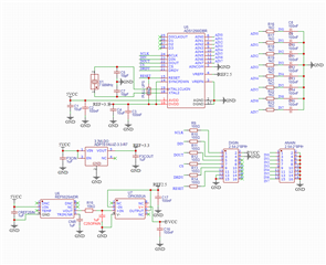
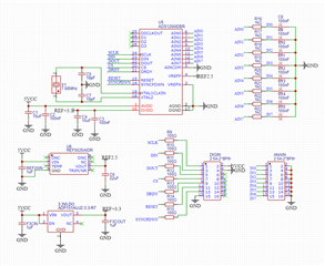
This is the schematic I designed. Are there any areas that appear to be unreasonable or in need of correction?
My signal ranges from 0 to 20 Hz with a sampling rate of 200 Hz.
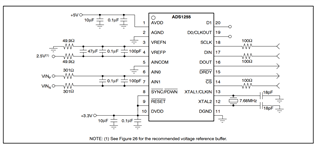
The following is the circuit diagram provided in the ADS1256 datasheet. I would like to know why there are so many decoupling capacitors connected to the VREF pin and their purpose.
Hi LEO_0916,
Some thoughts about your schematic:
-Bryan
Thank you very much for your assistance. I have made modifications to the circuit, please help me check if it is correct. By the way, I only need external control for the RESET pin, so is it sufficient to add a pull-up resistor to the RESET pin?
Hi LEO_0916,
This looks like you made all of the changes we recommended, so that is a good start
Regarding your question: even if you do not connect anything to the SYNC/PWDN pin, you can still issue the SYNC command to synchronize the conversion. So that functionality is still available to you, just by command and not using the pin.
-Bryan
HI LEO_0916,
I am glad we could help you resolve your issue quickly
-Bryan