This thread has been locked.

If you have a related question, please click the "Ask a related question" button in the top right corner. The newly created question will be automatically linked to this question.

ADS1115 Conversion issues

Other Parts Discussed in Thread: ADS1115

I have attempted to set up a single ended conversion using single-shot mode but am receiving the same value no matter the input (0x7FFF). Also before I start a single shot I read the conversion register and it is not 0 as stated in the data sheet, instead it is the same value as after I attempt to start a read. What gives?

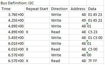
 here is my i2c communication:

here is the sequence:
init the config registers of two ADS1115 chips (set to single shot mode)
read the config register of device 0x48 to see if the OS bit is set indicating the device is idle
if idle, write to the config register with OS = 1 to trigger a single shot read
Read the config register to see if the conversion is complete by seeing if the OS bit is set
if finished, read the conversion register

  • Realized I wasn't disabling the comparator when I triggered the single shot read. Now the conversion register is changing according to the input value.

    How do I translate the conversion value to a voltage?

    Thanks

  • Ryan,

    Welcome to the forums!  The inputs generally measure a differential voltage, so you can get a +/- reading over the full-scale range (binary two's complement.)  So one code (LSB) is 4.096V/PGA/2^15 volts (see Table 4 in the datasheet.)  So if you multiply the number of codes (returned result) times the LSB size you will get the result in volts.

    If you measure single-ended you will only get the positive range of values (0x0000-0x7FFF.)  Something else to note is that your inputs can never exceed the supply voltage by more than 300mV even if the full-scale range increases to above the supply range.  The same is true with ground.  You can't input a negative voltage more than -300mV from ground.

    Best regards,

    Bob B

  • Bob,

    Can we guarantee a correct reading if we only bias 100 mV (not more than 300mV) on the negative input pin in differential mode?

    Thanks!


  • Richard,

    The normal input range of the device is GND to VDD.  The absolute maximum input range is 0.3V below GND to 0.3V above ground.  The device will measure signals above and below the supply rails, as long as the absolute maximums are not exceeded.

    Best regards,

    Bob B

  • Excellent sir!

    Thank you.

  • Hi, Bob,

    I am reading ADS1115's datasheet, and want to know following questions:

    1. what is the FS input range when ADS1115 is powered by 3.3V or below? If I want to achieve +-4.096V FS input, must I use 4V powered ADS1115? 

    2. What is the exact reference voltage value inside the ADS1115? Will it change when ADS1115 is powered by different voltage?

    Thanks for  your kind relpy.

    B. Regards,

    Frank

  • Hi Frank,

    The maximum input voltage that can be applied to the device must not exceed the VDD supply; however, the device will output conversions according to the full-scale selected  +/-4.096V/PGA.  The ADS1115 internal reference architecture does not work in the same fashion as a traditional voltage reference; in other words, if you were to open the device you will not find an actual node that measures the voltage reference 4.096V. The device will still provide conversions with the +/-4.096V Full-Scale at VDD=3.3V.  The "virtual" reference does not change and the Full Scale is still 4.096V; even if the supply is lower than the full-scale value.  The internal reference operates differently from other ADC's.   The easiest way to think about this device is in terms of the scale voltages available:  +/-0.256 to +/-6.144V; where the device provides conversions proportional to these virtual full-scale values; in other words, these scales express the full-scale range in the ADC conversion.  The value of the reference does not change with VDD supply, so for example, you could set the full-scale as +/-4.096V, and have a VDD=3.3V and the device will provide the conversions as the full-scale setting.

    -->The important thing to consider is that the voltage at the inputs of the ADS1115 should not exceed the VDD supply; according to the Absolute Maximum Rating table, the inputs should never exceed VDD+0.3V...   Also, when the device is at maximum supply of VDD=5.5V, the inputs can not exceed 5.5V.  However, the device will still provide conversions proportional to the virtual full-scale value (+/-4.096V/PGA).

    Thank you and Best Regards,

    Luis

  • Luis,

    Thanks so much!

    So, if my ADS1115 is 3.3V powered, and I set PGA=1, I will not fully utilize the +/-4.096V full scale input, right?   

    Another question is even we have +/-6.144V full scale input range when PGA = 2/3, but it seems we can never fully utilize the +/-6.144V FS, as the largest differential Vin is +/-5.5v when ADS1115 is 5.5V powered, right?

    Frank


  • Hi Frank,

    Yes, you are correct.  When VDD=3.3V; you can only apply a maximum input signal of 3.3V.  The device could be set to the +/-4.096V scale and the device will provide output conversions proportional to the +/-4.096V scale setting.  The same case occurs when VDD=5.5V; a maximum input voltage signal of 5.5V may be applied; the device could be set to provide output conversions proportional to the +/-6.144V scale setting; however, the user will never reach the +/-6.144V full scale.

    Thank you and Best Regards,

    Luis