This thread has been locked.

If you have a related question, please click the "Ask a related question" button in the top right corner. The newly created question will be automatically linked to this question.

ADS1263: 3 wire RTD conversion doesn't match calculation/measurements

Part Number: ADS1263


Hello,

I'm trying to use the ADS1263 for a 3-wire RTD measurement with the same circuit as proposed in the component's datasheet as a typical application (image below).

The conversion value does move accordingly with temperature variations, however the conversion value doesn't match neither the measured resistances nor measured voltages of the active circuit.

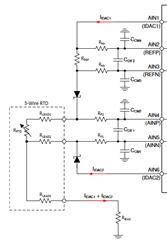
I'm using a reference resistor with nominal value Rref=8kΩ and a platinum RTD with Rrtd=500Ω at 0°C. Measuring the actual resistances I found Rref=7.967kΩ and Rrtd=544Ω.

As I'm using a PGA gain of 8, I expect a conversion C=(Rrtd*8/Rref)*2^32, which should give me a conversion of roughly 0x8BXXXXXX. However the what I actually get from the ADS is 0x38XXXXXX.

I also measured Vref=1.967V and Vrtd=0.135V, which seem to confirm the calculations above.

The ADS register configuration is as follows:

reg_power = 0x01

reg_interface = 0x02

reg_mode0 = 0x30

reg_mode1 = 0x80

reg_mode2 = 0x35

reg_inpmux = 0x45

reg_idacmux = 0x61

reg_idacmag = 0x33

reg_refmux = 0x22

Before starting the acquisition I set reg_inpmux = 0x23 perform a full-scale calibration.

I have tried playing around with many settings but I cannot figure out what the issue is.

Would anybody have an idea? Thanks in advance.

  • Hi l r,

    Can you send me a schematic of the input structure and the ADC so we can review? You can post images directly into the e2e thread or attach images using the "Insert" dropdown at the bottom of the post window

    Also, the ADC has a binary twos complement coding scheme (see Table 9-19 in the datasheet), so your equation should be C=(Rrtd*8/Rref)*2^31. This will give you a code around 0x45xxxxxx. So your data is still off, but not by quite as much as you originally calculated

    -Bryan

  • Hello Brian,

    I indeed missed this important detail, thanks for pointing that out.

    Here's the schematics for the RTD ADC part of my board (Rref is 7.5kΩ in the schematics but I'm actually using 8kΩ):

  • Hi l r,

    Thanks for sending the schematic. One thing I noticed is that you have REFMUX = 0x22 = 0010 0010b

    This translates to RMXUP = 100 and RMUXN = 010, which selects RMXUP = AVDD and RMUXN = AIN3

    You should change this to REFMUX = 0x12 = 0001 0010b, so RMUXP = AIN2. Let me know if this helps

    -Bryan

  • Hi Bryan,

    Thank you for your response.

    It turns out I am actually setting REFMUX=0x12.

    I'm really sorry I was lazy when making the post and translated register values in my head instead of recovering them from the code since I'm using enums. I have now doubled checked the other ones and they're all good.

  • Hi l r,

    You should also check that the PGA common-mode range is being respected. This is given by equation 12 in the datasheet.

    You can also visualize this behavior using the "PGA1 input range" tool our Excel based calculator: https://www.ti.com/tool/download/ADS126X-CALC-TOOL

    When I put in the values from your circuit into this tool, I am getting an error on the PGA_N output. You need to increase the value of the bias resistor (R37) to shift the absolute voltage on each pin into the PGA's VCM range. It seems like increasing R37 to 2kohm should be sufficient, but I leave the final determination to you

    -Bryan

  • Bryan,

    Thanks for the suggestion.

    I tried changing Rbias to 3kΩ or even overshooting it to 12kΩ (values I had available), but unfortunately this didn't affect the conversion code.

  • Hi l r,

    You should not change RBIAS to 12kohm, this would likely make things worse because the voltage across RBIAS will be 6V. Since this is not possible, the IDAC current will start to sag and the behavior will become uncertain. However, 3kohm should have improved the situation if the PGA VCM range was the actual issue. You should still change RBIAS to be >1.5kohm however

    I tested this on my EVM using your same connections, as well as 250uA current sources, a 501 ohm resistor as the input, 8kohm as RREF, and 2kohm as RBIAS. I measured 124.7 mV across the inputs using my DMM and the resulting measured data using the GUI was 124.697mV. So this circuit works with the ADS1263, which means there must be something we are missing with your design

    I noticed that you have a mismatch in your register settings in that you have selected the FIR filter as well as the 50 SPS data rate. Note that the FIR filter only accommodates data rates up to 20 SPS, so you will either need to change your filter type or your data rate. This shouldn't have caused an issue though because the ADC internal logic will default one way (I cannot recall which off of the top of my head, but you are either running at 20SPS and FIR filter or 50 SPS and sinc1 filter. You could measure between DRDY pulses to confirm)

    I also noticed that you have both input chop and IDAC rotation enabled. Can you disable these and take additional measurements?

    -Bryan

  • Bryan,

    Indeed this is strange, we must be missing something. An important remark is that I have 3 prototypes of the same board, and they all give me the same conversion code (~0x38xxxxxx), so it's unlikely to be due to faulty components.

    I originally had a sinc4 filter, but I noticed I was missing frames so I changed to FIR. I would imagine that it defaults to sinc1 because I'm still receiving DRDY interrupts at 50SPS.

    Disabling input chop and IDAC rotation also doesn't seem to change anything...

  • Hi l r,

    Can you let me know what are the actual ADC codes you are reading? If you want to send me a data dump of 1000 samples or so, that would be great. You can attach an Excel file using the "Insert" dropdown at the bottom of this window

    I see that you are performing gain calibration prior to your measurements, can you let me know what value the SYSGCAL command stores in the FSC registers?

    -Bryan

  • Bryan,

    Here's a csv log in hex of 1500+ continuous samples I got from the ADC. The FSCAL values I read were the following:

    FSCAL0 = 0x0d

    FSCAL1 = 0x6b

    FSCAL2 = 0x33

    adc_conv_log.csv

  • Hi l r,

    That FSC value translates 0x336B0D = 3369741d. Compared to the nominal value (0x400000), that amounts to a scaling factor of ~0.8. This seems way too low, I would have expected something like 0.995 to compensate for the gain error.

    Your expected code is C=(Rrtd*8/Rref)*2^31 = (544*8 / 7967)*2^31 = 0x45EBA0C2. If you multiply this by your FSC scaling value, you get 0x382CB83F, which is approximately the code values you reported in your excel sheet. 

    Can you return the FSC value back to the nominal (0x400000) and see if you get the expected results?

    -Bryan

  • Bryan,

    That was it thanks a lot!

    I stopped performing a full-scale calibration and now the conversion values are within the expected range. I had already tried doing that at some point but I guess I did something wrong on this test.

    So finally should I not perform a full-scale calibration or am I not doing the correct process? I was setting the inputs to Vref (AIN2 and AIN3) before performing the calibration.

  • Hi l r,

    I am glad we were finally able to resolve this issue

    I am not sure why the FSC did not work for you, when I performed it on the EVM using the same conditions I got a value that was closer to 0.995 as mentioned.

    You might try rerunning the FSC and making sure that all of the correct settings are applied first. When I originally ran FSC on the EVM I got the wrong code because I forgot to switch the gain to 1 when using the voltage across RREF as both the VREF and analog inputs.

    Also note that if you are using a gain of 8, it would make more sense to calibrate using a full-scale voltage at a gain of 8, not gain of 1.

    -Bryan