This thread has been locked.

If you have a related question, please click the "Ask a related question" button in the top right corner. The newly created question will be automatically linked to this question.

DAC81416EVM: DAC channels not getting updated

Part Number: DAC81416EVM

Hi,

I am using teensy 4.1 controller to initiate SPI communication with the DAC 81416 EVM board and send the values '65535' and '0' to DAC channel 0. 

The connections are as follows:

Teensy Pin 6 (CS) - J8.2

Teensy Pin 11 (SDI) - J8.4

Teensy Pin 12 (SDO) - J8.3

Teensy Pin 13 (SCLK) - J8.8

Teensy Pin 6 (3.3V) - J8.5

Teensy GND - J8.6

On J7 I give power supply as follows:

J7.3 - GND

J7.5 - VCC/VAA - 5 V

J7.6 - VSS - -15 V

J7.7 - VCC - +15V

The jumper configurations on the EVM board are as follows:

J2 - Open

J3 - Open

J9 - Closed

J10  - 1-2: 3.3 V on J8.5 (from teensy 4.1)

J11 - 1-2: VREF from REF5025

J12 - 2-3: VSS on J7.6 (-15 V)

I am using the following code:

***********************************************************************************************************************

#include <Arduino.h>
#include <SPI.h>  // include the new SPI library:

const int CS = 6;


inline void CSON()
{
  digitalWrite(CS, LOW);
}
inline void CSOFF()
{
  digitalWrite(CS, HIGH);
}

void write_reg(uint8_t reg, uint16_t wdata)
{
  uint8_t lsb = ((uint16_t)wdata >> 0) & 0xFF;
  uint8_t msb = ((uint16_t)wdata >> 8) & 0xFF;
  
  SPI.beginTransaction(SPISettings(16000, MSBFIRST, SPI_MODE1));
  //SPI.setClockDivider(SPI_CLOCK_DIV64);
  CSON();
  delayMicroseconds(10);
  //Serial.println("Hier");
  SPI.transfer(reg);
  //Serial.println("und hier?");
  SPI.transfer(msb);
  SPI.transfer(lsb);
  CSOFF();
  delayMicroseconds(10);
  SPI.endTransaction();
}

void setup()
{
  Serial.begin(9600);
  pinMode(CS,OUTPUT);
  pinMode(11,INPUT);
  pinMode(12,OUTPUT);
  pinMode(13,OUTPUT);
  digitalWrite(CS,HIGH);
  //delay(5000);
  SPI.begin();
  delay(1000);
  write_reg(0x03, 0x0084); // SPICONFIG: DEV-PWDWN=0
  write_reg(0x04, 0x00FC); // GENCONFIG: REF-PWDWN=0
  write_reg(0x05, 0x0000); // BRDCONFIG: DACx-BRDCAST-EN=0
  write_reg(0x06, 0x0000); // BRDCONFIG: DACx-SYNC-EN=0
  write_reg(0x09, 0x0000); // DACPWDWN: DACx-PWDWN=0, x={A,B,C,D}
  write_reg(0x0A, 0x0000); // DACx-RANGE=0b0000, i.e. 0-5V
  write_reg(0x0B, 0x0000); // DACx-RANGE=0b0000, i.e. 0-5V
  write_reg(0x0C, 0x0000); // DACx-RANGE=0b0000, i.e. 0-5V
  write_reg(0x0D, 0x0000); // DACx-RANGE=0b0000, i.e. 0-5V
  delay(1000);
  //DAC initialize
  write_reg(0x10, 0xFFFF);   // DAC-A(mid code)
  write_reg(0x11, 0xFFFF); // DAC-B(full code)
  write_reg(0x12, 0xFFFF); // DAC-B(full code)
  write_reg(0x13, 0xFFFF); // DAC-B(full code)
  write_reg(0x14, 0xFFFF); // DAC-B(full code)
  write_reg(0x15, 0xFFFF); // DAC-B(full code)
  write_reg(0x16, 0xFFFF); // DAC-B(full code)
  write_reg(0x17, 0xFFFF); // DAC-B(full code)
  write_reg(0x18, 0xFFFF); // DAC-B(full code)
  write_reg(0x19, 0xFFFF); // DAC-B(full code)
  write_reg(0x1A, 0xFFFF); // DAC-B(full code)
  write_reg(0x1B, 0xFFFF); // DAC-B(full code)
  write_reg(0x1C, 0xFFFF); // DAC-B(full code)
  write_reg(0x1D, 0xFFFF); // DAC-B(full code)
  write_reg(0x1E, 0xFFFF); // DAC-B(full code)
  write_reg(0x1F, 0xFFFF); // DAC-B(full code)
}

void loop()
{
  // Channel 1 is made HIGH for 1 sec and then LOW

  write_reg(0x10, 65535);
  delay(1000);
  write_reg(0x10,0);
  delay(1000);

  Serial.println("Loop done");
}
********************************************************************************************************************

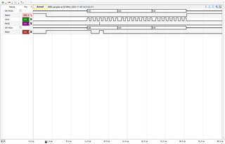
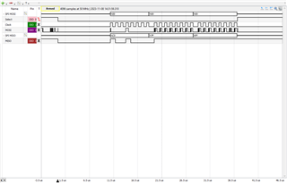
 I can see the SPI signals when I check it on the testpoints TP6,7,8,10.

But I do not see any outut on the DAC channels. 

Attached here also the screenshot of the logic analyser's output (where the addresses and values are not coming out accurate, for some reason)

Please let me know why this issue is occuring. 

Thank you :)

  • Hi Lalita, 

    Can you remove the jumper on J11 and write only the command to power up the internal reference. Please also measure the SPI signals during that command with a scope and share a screenshot. Check the REF pin to see if the internal reference powers up. If this command is not being seen correctly on the scope then there could be a problem with your SPI library that you will have to debug first. You can also measure the SPI signals without them connected to the EVM to verify that they have the right format first. 

    Best,

    Katlynne Jones 

  • This is the screenshot of the SPI outputs sent from the controller:
    The first 2 images are the SPI outputs as seen at the controller side The oscilloscope readings are for MISO (blue) and CS(Yellow).
    The last 2 images are the SPI outputs when DAC's internal reference is activated in the code by setting the bit 14 of Gen Config Register as 0. J11 is left open. When I measured the voltage at J1.7, it showed 2.5 V.


  • Hi Lalita, 

    Just to confirm, are you able to toggle the reference and see the 2.5-V on J1.7 go on and off if you write multiple commands to set bit 14 in GEN CONFIG to 0 and 1? Your screenshots don't really convey that the right command is being sent, but it will be good to know that you are able to control the reference. It would also be helpful if you could annotate the screenshots with what command is being sent. Right now, I don't want to look at the MISO (SDO - serial data out from the DAC) line until it's been confirmed that you are able to write to the DAC successfully through the MOSI (SDI - serial data in from the DAC) line. 

    Best,

    Katlynne Jones

  • Hi Katlynne, 

    I understood what you meant now. The reference pin on my DAC EVM board is not going low at all whether I write 0 or 1 to the Gen Config register. It’s always showing 2.5 V. 

  • Hi Lalita, 

    So from this it seems like you SPI writes are not working. Can you write the following commands and send another screenshot of each command with the SCLK and SDI pin shown on the scope and SCLK, SYNC, and SDI shown on the logic analyzer? Try to zoom in so the write takes up the whole window in each screenshot (SYNC falling edge to SYNC rising edge). 

    register 0x03, data 0x0040

    register 0x04, data 0x0000

    check reference level

    register 0x04, data 0x0400

    check reference level

    register 0x04, data 0x0000

    check reference level

    register 0x05, data 0x5555

    This last command is just to help us see that your controller is sending the right data. The SDI pin should be toggling low and high on each clock to send data 0x5555. 

    Best,

    Katlynne Jones 

  • register 0x04, data 0x0000

    check reference level

    register 0x04, data 0x0400

    check reference level

    Can you please explain to me once, what exactly we are doing here ? From the data sheet, this means Gen Config register 's bit 10 is made 0, reference level checked, then bit 10 made 1, reference level checked. However, this is one of the reserved bits of that register.

    Also, if you look at my code, I had made a mistake earlier with programming the GEN CONFIG Register that I noticed now. That was the reason why I was not able to control the reference. Now, after I send the right values to the register, my reference is actually toggling to 2.5 V and 0 V.

  • Hi Lalita,


    Looks like your SPI communication is working as you are able to toggle the internal reference of the DAC81416.

    Please follow the instruction to check the basis functionality of the DAC81416 as described below-

    A. Power cycle the EVM power supply and measure the supply voltage on TP4, TP5, TP11 and TP13

    B. write these values in the corresponding reg - 

         1. Write 0x0A04 in SPICONFIG (0x03) -  to power-up the DAC81416 device 

         2. Write 0x7F00 in GENCONFIG (0x04) -  you can use on board REF5025 reference or write 0x3F00 to enable the internal reference of the DAC81416                  (J11 > pin[1-2] - open this while enabling the internal reference of the DAC81416)

         3. Write 0x0000 in DACPWDN (0X09) - to power-up the individual DAC channels

         4. Write 0x8000 in DACn_DATA (n = 0x10 to 0x1F) -  to configure the individual DAC channel outputs to 2.5 V (default output voltage range for all the channels is 0 V- 5 V)


    C. If you are still not able to see any output on the DAC channels, please refer to the section 7.6 Timing Requirements of DAC81416 data sheet 


    Let us know if you are still not able to configure the DAC channels output voltage.


    Thanks,

    Sanjay

  • Thank you for your feedback. Looks like there was a problem with my evaluation board, but when I tried the same thing on a new board it worked.