This thread has been locked.

If you have a related question, please click the "Ask a related question" button in the top right corner. The newly created question will be automatically linked to this question.

ADS54J60EVM: Unexplained DC offset

Part Number: ADS54J60EVM
Other Parts Discussed in Thread: LMK04828

Hi everyone,

We are facing a strange issue with our ADS54J60EVM FMC ADC. While sampling our input signal that varies from 20mVpp up to 1.9Vpp (the maximum swing that should in theory give us the full scale of the ADC) we are seeing at roughly 50% of the time DC bias/offset.

Please refer to the FFT spectra below. In the "problematic" one we can clearly see that the SNR diminishes due to the DC offset while the other one shows normal operation.

As we want to extract the frequency content from the 10MHz - 120MHz range, this is very problematic and difficult to resolve in processing.

The input signal normally does not feature a DC content (if any, it may be at max 10mV). Even if it had a DC content though, shouldn't the passive balun cut it out?

Could this behavior be a due to a malfunction of the DC offset correction block? We have not disabled it, so it should be enabled by default.

https://e2e.ti.com/support/data-converters-group/data-converters/f/data-converters-forum/716690/ads54j40-ads54j40-interleaving-offset-correction-how-to-freeze

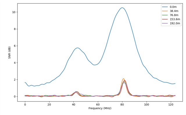
We are also seeing interleaving spurs, even if we only give a stable 80MHz input RF frequency. We do not know if this can be avoided.

What do we have to do? Do we have have to use a high pass filter to cut off the DC content completely? Do we have to use a low pass filter to cut above 120MHz? Do we have to use an SMA DC blocking capacitor? We are still trying to figure out if this should be expected or not.

  • Hi Anastasios,

    I will look into this for you. Can you please provide a few more details?

    Can you please share what you are using for your input signal and the input frequency (80 MHz). 

    Can you also please clarify what the different traces in the plots are? What is the legend distinguishing?

    Best regards,

    Drew

  • Hi Anastasios,

    Please verify that you are using our ADS54J60EVM?

    Could you also please send us FFTs for the above traces (with amplitude as the y-axis)?

    In the meantime, I would also recommend checking out this apps note about the dc correction block in this part:

    https://www.ti.com/lit/an/sbaa576a/sbaa576a.pdf?ts=1699476778588&ref_url=https%253A%252F%252Fwww.google.com%252F#:~:text=Per%20the%20ADS54J60%20user%20guide,clocking%20chip)%20and%20the%20ADC.&text=By%20default%2C%20the%20DC%20offset,visible%20above%20the%20noise%20floor.

    Best regards,

    Drew

  • Hi Drew,

    we are indeed using ADS54J60EVM on the FMC connector of a Xilinx ZCU102 FPGA.

    The input signal is the output of an RF generator plus a mixer to simulate AWGN.

    The above spectra are the result of the FFT accumulation over 1sec, the FFT size is N=1024 and it also features a zero-padding function (that is: only 64 samples that are fed into the FFT core are non-zero, the rest are zero).

    To make sense of the legend, the meters refer to the estimated "distance" from the source. So in our RF generator we are providing higher Vpp of the sine wave for the blue waveform, then lower for orange, slightly lower for green etc. This power switching behavior is repeated again and again with 10KHz rate.

    The only time when Vpp is close to 1.9V is on the "blue" waveform. On the rest of the waveforms Vpp is closer to 20mVpp-100mVpp.

    Our question is: does this happen because the ADC operates on AC-coupled mode? As I said previously, our signal has negligible DC bias. But we cannot really set it to work on DC-coupled mode, as we would have to physically modify the ADS54J60EVM board. Is this right?

    I also researched the DC correction block and I found that another TI user had faced a similar issue on a different ADC. He resolved it by disabling it completely.

    PS. The peak close to 40MHz is an interleaving spur and not a harmonic.

  • Hi Anastasios,

    Thank you for all the details, However, we are still not clear on a few things as we are not used to looking at data in this format....

    Is this the problematic plot?

    If so, then yes, it would be suggested to disable the DC correction block in the ADC and retake the data to see if this helps.

    Is that how you were able to achieve this plot? Which seems better?

    To answer your question: Our question is: does this happen because the ADC operates on AC-coupled mode? RR: no, the ADC is inherently DC coupled, meaning it can accept AC or DC coupled signals. The EVM by default should have an passive balun frontend and therefore would be inherently AC coupled, DC blocked. As I said previously, our signal has negligible DC bias. But we cannot really set it to work on DC-coupled mode, as we would have to physically modify the ADS54J60EVM board. Is this right? RR: you can use a DC blocking cap if you feel this might help in your test setup, but as stated above the EVM already has a blocking DC blocking cap on the analog input frontend.

    Regards,

    Rob

  • The problematic plot is the one where the SNR of the DC FFT bin (frequency 0Hz) is near 30 dB.

    No, we didn't change anything regarding the ADC configuration. Our system was running for over 1 hour and at random times the FFT would give "unexplained" DC offset, thus ruining our output data.

    To rule out a bug in our system, we used an internal "simulated" ADC block which provided raw samples (similar to the input pattern of a DAC). There was no DC offset in that experiment.

    This is why we assume that the DC correction block works OK at some point but after some time something happens and provides completely wrong raw data.

  • Hi Anastasios,

    Per your last comment: This is why we assume that the DC correction block works OK at some point but after some time something happens and provides completely wrong raw data.

    Is there anything in the system changing? For example, frequency or sampling rate of the ADC? Any supply voltages, etc?

    Thanks,

    Rob

  • Hi Rob,

    The sampling rate should not change as it is derived from the LMK04828 block. Also the supply voltage is provided by a high quality 5V DC adapter, tested to be perfectly at 5V using an oscilloscope.

    The only thing that changes is the amplitude of the input signal to the A_INP SMA port. The ADS54J60EVM board is not actively cooled though so in that respect we do not know if this plays a role.

    Tasos

  • Hi Tasos,

    I think your last statement is key. Are you letting your board sufficiently thermal soak before the ADCs calibration routing is set?

    If not, and the ADC is calibrated at power up, the heat of the board and ADC will change, and the ADCs calibration will no longer be valid or appropriate.

    Can you please try calibrating the ADC after the board is thermally uniform. And then see if you get changes in amplitude?

    Also, have you tried to disable the calibration block altogether? I don't see if you have tried that above, sorry if I missed this.

    Regards,

    Rob