Need help with reading back A/D inputs on TLA2528 component.
Background: Have part configured for channels 0-3 as A/Ds and channels 4-7 are GPIO outputs. We are successfully communicating with the GPIO outputs (can toggle outputs from logic "0" to logic "1" and back but can't seem to read the A/D inputs).
The initialization routine that we are using is as follows:
Write to GENERAL_CFG register 0x00
Write to DATA_CFG register 0x0F
Write to OSR_CFG register 0x00
Write to SEQUENCE_CFG register 0x00 (Manual sequence)
Write to PIN_CFG register 0xF0 (Chs0-3 A/Ds & Chs 4-7 GPIO)
Write to GPIO_CFG register 0xF0) (CHs 4-7 digital outputs)
Write to GPO_DRIVE_CFG 0xF0 (Chs 4-7 as open drain outputs)
Write to GPO_VALUE register 0xF0 ( To set GPIO outputs to logic"1")
This completes the initialization routine.
Procedure for trying to read A/D inputs:
Write to CHANNEL_SEL register 0X02 (To select A/D input on channel specific channel)
Read data being outputted by device
Problem: Issue is data is inconsistent and not the expected values for the actual A/D input voltage.
Suspect we are not properly configuring device or not executing the read command correctly. Can you advise?
Problem 2:
On the GPIO outputs that we have configured as open drain the outputs are pulled up to +5 volts via a 10K resistor but outputs are only going up to 3.7 volts. We have removed all loads on these outputs except for the 10 k pullup resistor. The TLA 2528 AVDD and DVDD power lines are both tied to a 3.3 volt supply and each supply input is bypassed with a 1 uF cap close to input pins.
Any suggestions on this issue?
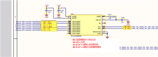
Snap Shot of schematic: