This thread has been locked.

If you have a related question, please click the "Ask a related question" button in the top right corner. The newly created question will be automatically linked to this question.

ADC09QJ1300:How to extract samples from JESD204C IP output data

Part Number: ADC09QJ1300

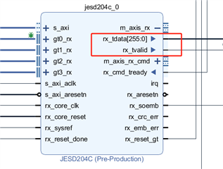
Hello, I used Xilinx FPGA and ADC09QJ1300 to complete the design of JESD204C. At present, I can see the IP output data of JESD204C of Xilinx in Vivado.
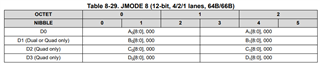
As shown in the figure, I use JMODE 8, and the output port of IP is a 256bit of data. As far as I know, in this 256bit, each channel takes up 64bit.


But I still don't know how to extract the samples in the 64Bit of each channel. I checked the [8.4.2.1 JESD204C Transport Layer Data Formats] section of the data manual, but I still don't understand how to process the data.
I want to get a clear indication, such as which bits to which in the 64bit data is sample information.
I have been reading it for many days, but I still don't understand it, so I came to ask for help, thank you very much for your help

  • Hello,

    Have you taken a look at table 8-29 of the datasheet. This shows how the data gets packed into the JESD structure. See the picture below.

    From this we can see that there are 4 lanes, each lane has one channels worth of data so for instance there are three total octets for a total of 24 bits, in that there are 6 nibbles. Then for Channel A for example that will appear on lane D0. First comes sample A0 and only the first 9 bits are actual data the next three bits will be 000, this is because 9 bits is a bit of a strange number so we need to pad the sample to get to 12 bits, then the next sample will come A1 and the same as before only the first 9 bits are data the next three are 000. This process can be continued for the next three channels worth of data.

    One other test you could perform is to put the ADC into transport layer test pattern mode by programming the JTEST register (0x205) to a value of 0x05, this will cause the ADC to output a constant signal to the FPGA and from there you can check that your samples match what is seen in table 8-46. You should see this pattern repeated across all 4 lanes. This will also help to tell where on sample starts and the next begins.

    best,

    Eric Kleckner

  • Thank you very much for your reply. I have read the sample data