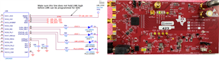
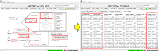
Hi :
PIC1 is setting that i uesd to my design.
i used onboard clock.
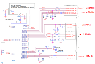
PIC2 is output signal form LMK04828 Which output clock to FPGA and ADC32RF45.
My question is PIC3 LMK04828 output state that all the LED should be turn on?
If the only PLL2_LOCKED's LED turns on . is it correct?
pic1 :
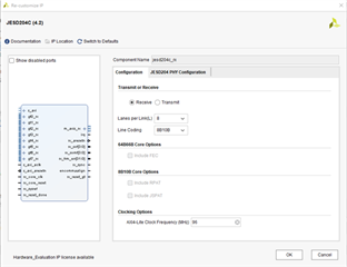
pic2 :
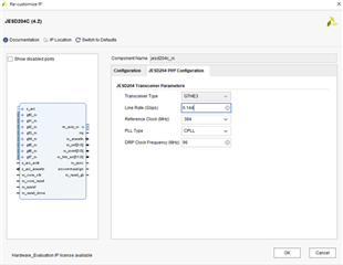
pic3 :