This thread has been locked.

If you have a related question, please click the "Ask a related question" button in the top right corner. The newly created question will be automatically linked to this question.

ADS1278: ADS1278 Testing

Part Number: ADS1278

Greetings,

I'm a beginner to ADC, I have ADS1278 I wanted to learn interfacing the ADC with FPGA

but before that i wanted to learn how it is working ?? i have digilent how can i test that IC with logic analyser i just drew a line diagram and motioned below

please let me know what are all the mistake i'm making

Best regards,

Tex

  • Hello Tex,

    Can you provide a schematic of your breakout board?  Also, please let me know how the device is configured, SPI or Frame Sync.

    For expected timing, please look at the SPI Format Timing diagram section of the datasheet.  In SPI mode, CLK, SCLK, and DIN are all ADC inputs, and /DRDY and DOUT are outputs.

    Regards,
    Keith Nicholas
    Precision ADC Applications

  • Hi Nicholas,

    i don't have the schematic right now but it is connected to the same pins of ADS1278.. 

    i haven't went to the programming part for data processing actually but i just generated sclk from the controller and gave required inputs to the IC 

    reviewed SPI format timing diagram and gave inputs as u can see in the image,

    The output in the scope are,

    Dout 200Hz, DRDY 200Hz & SYNC 200Hz 

    drdy should go low and high for every 24 bits as per my understanding

    Please tell me what mistake am i doing right now 

    Best regards,

    Tex

  • Hi Tex,

    This a holiday week in the US, we will respond to you next week. Thanks for your patience

    -Bryan

  • Hello Tex,

    The FPGA needs to monitor the /DRDY output from the ADS1278.  When /DRDY transitions from high to low, data are ready to be read from the ADC.  

    CLK needs to be a continuous signal; the SCLK will idle in the low state.  When /DRDY goes low, the FPGA will then generate 24 SCLKs, and the 24b conversion result will be on the DOUT pin.

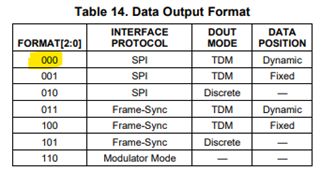
    When using SPI, the most common configuration is TDM mode, where all ADC channels are shifted out on the DOUT1 pin.  In this case, the total number of SCLKs will be 8*24=192 for each SPI frame.  The FORMAT pins need to be connected to ground to support this mode.

    Here is the order of operation.

    1. Monitor the /DRDY pin, wait for /DRDY to go from high to low.

    2.  Send 192 SCLKs, read data on DOUT1 pin.

    3.  After data has been read, wait for the next /DRDY transition from high to low.

    Assuming CLK=27MHz, SCLK can also be set to 27MHz.  This will support data rates up to 105468 sps.

    The SYNC pin should be held high under normal use.  The SYNC pin functions as an ADC reset and should only be used to re-synchronize the ADC after power-up and after any mode change.

    I will need to see a sketch showing all pin connections of the ADS1278 to further help.  Also, a waveform plot showing the CLK, SCLK, /DRDY and DOUT1 signals, will also help.

    Regards,
    Keith

  • Hi keith,

    I'm using 001 Fixed tdm SPI format,

    i'm trying to get 200 samples in 1 hz sine wave,

    as u said drdy signal should go high to low 24 clk cycles 

    Both DRDY and Dout showing same output..

    My connections are.. for 200 samples

    sclk: 102400, clk: 102400, vdd: 3.3V

    Please tell me what are all the mistakes am i doing..

    Best regards,

    Tex

  • Hi Tex,

    What is the frequency of DRDY in the attached image?  I assume it is 200Hz?  In addition, all IO signals should be at the level of IOVDD, or 3.3V.  Is DRDY 3.3V?

    Also, please provide a scope capture of DRDY and SCLK to ensure the timing between these two signals is correct.

    I would also suggest that you verify all supply voltages and pin connections to the ADS1278.

    AVDD 4.75V to 5.25V

    DVDD 1.65V to 1.95V

    IOVDD 1.65V to 3.6V  (I assume this is 3.3V)

    If you can provide a screenshot of the ADS1278 schematic, I will review it to confirm everything is connected properly.

    Regards,
    Keith

  • Hello Keith,

    It is working now,

    As you said issues was in the Firmware code 

    Best regards,

    Tex

  • Hi Tex,

    SCLK needs to be at a much higher frequency than DRDY in order to read the data in less than one sample period.  You had stated that SCLK was set to 102400 (same as CLK frequency).  You need to update your firmware/code to fix this in order to correctly read the data from the ADC.

    Regards,
    Keith