This thread has been locked.

If you have a related question, please click the "Ask a related question" button in the top right corner. The newly created question will be automatically linked to this question.

ADS4249: Reference Clock noise at the RF IN port

Part Number: ADS4249

Hello,

My customer is testing a board they designed using the ADS4249.

They say that the reference clock of 245.76MHz is observed at the RF IN port of ADS4249.

In what cases can symptom like this occur?

Is there a way to reduce the reference clock noise level at the RF IN port?

Thank you.

JH

  • Hi JH,

    If the CLK and RF INs were routed on the same layer of the PCB, then the CLK is coupling to the RF IN lines.  It is recommended to route the CLK on a different layer from the RF INs then via it up close the device to minimize any possible cross talk on the board.

    Regards,

    Geoff

  • Hi JH,

    Please let us know if this is the customer's own design or the TI EVM?

    If the customer can give us a few measurements to look at, this will output....FFT output spectrum or similar would be best.

    Thanks,

    Rob

  • Hi Geoff and Rob,

    Thanks for your reply.

    This symptom occurs on the ADS4249 board designed by the customer.

    They said that the CLK was routed on the BOT side and the RF line was routed on the TOP side.

    It was confirmed that when the CLK IC output level was reduced using a resistor, the CLK level at the RF IN port was reduced.

    I will check with the customer if they can provide the FFT output spectrum.

    Regards,

    JH

  • Hi JH,

    Yes, please share the customer's measurements on how the clock is being coupled to the analog inputs.

    This will help us get to the root cause.

    Thanks,

    Rob

  • Hi Rob,

    Here are the FFT capture images.

    Fs 245.76MHz, Fc 307.2MHz CW signal(Left: no signal / Right:CW)

    Thanks,

    JH

  • Hi JH,

    I don't see the clock signal in the FFT?

    I see the Fc frequency folding back at 60MHz, which is correct.

    thx,

    Rob

  • Hi Rob,

    Since the customer is using a sample rate of 245.76 MHz, the ADC output data above will have 245.76 MHz in the DC.

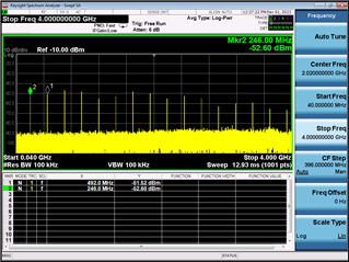
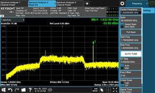
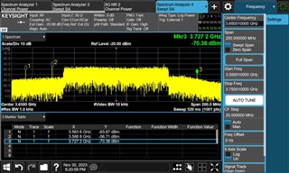
    Below is the SA captured image that the customer checked between RF Block and ADC RF IN.

    - Reference CLK signal (246.76MHz) x N signal output from ADC input

    - When this CLK signal and the LO signal of the system combine, a spur signal is generated near the output band, causing a problem that cannot be removed by a filter.

    1820MHz LTE                                                          3650MHz 5G NR


    Please advise on how to resolve this issue.

    Thanks,

    JH

  • HI JH,

    This is an unbuffered ADC, so this is to be expected.

    This won't corrupt the analog input signal being sampled.

    See figure in the datasheet below.

    Can you please get a copy of the customer's schematic?

    I would like to see if there is anything I can address here.

    Thanks,

    Rob

  • Hi Rob,

    Thanks for your help.

    I emailed the customer's schematic. Please review it.

    BR,

    JH

  • Hi JH,

    The schematic looks fine. I am still confused on what the customer is concerned about.

    Again, you will see clock frequency spurious using a spectrum analyzer probe at the analog inputs.

    This is inherent to the unbuffered ADCs internal sampling architecture. 

    In the captured data from the ADC, there should be no clock spurious....which I don't see above in the FFTs provided.

    Here is an app note that describes this behavior:

    www.analog.com/.../an-742.pdf

    Regards,

    Rob