Part Number: ADS52J90
Hello!
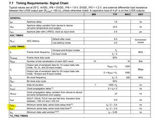
Looking at the datasheet for the ADS52J90, I can't seem to find a spec for the variance between the edge of the LVDS data clock and the data transition for the LVDS serial output channels. This is important for me to set up FPGA timing constraints and ensure I have a good enough data eye. Is this spec known for the ADS52J90, or can the minimum and maximum delays between clock edge and data transition be calculated from the other specs in the datasheet?
Thanks.