This thread has been locked.

If you have a related question, please click the "Ask a related question" button in the top right corner. The newly created question will be automatically linked to this question.

ADS1278: Cross-coupling or offset issue in differential inputs of ADS1278 with THS4521 buffers

Part Number: ADS1278
Other Parts Discussed in Thread: THS4521, , OPA2350, INA851, INA149, INA821, INA826, PGA855, THS4551, ADS1274

Hello,

I am facing a severe issue in one of my product designs with an ADS1278 and THS4521 buffers. It might very well be that I have misunderstood how to use both parts, but it would be important for me to verify if I can solve the problem or I have to rethink the concept from scratch.

In my application I have to measure several voltage drops from devices that are place in series. The issue that I face is, that when connecting more than one differential input to one of those components in series, the voltages read in the others change. The voltage change can not be explained solely by the input impedance of the single differential channels, as this influence should be marginal in my setup.

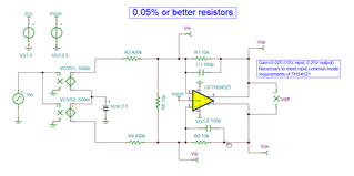
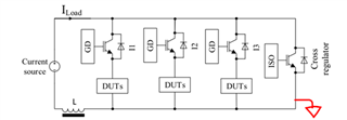
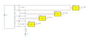
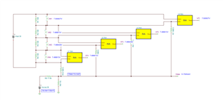
For debugging the issue I have build a very simple setup shown below:

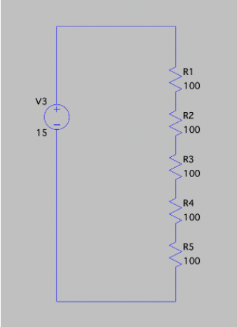
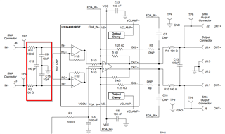
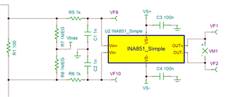
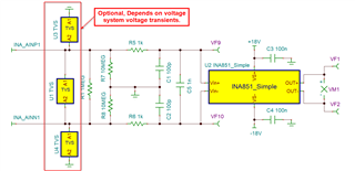
Simply 5 resistors in series, each one 100ohm and a voltage source of 15V. In this case the current flowing would be 30mA and the voltage drop in each resistor 3V. The THS4521 buffers are configured in a way that they attenuate the input signal, as they should be capable of reading up to 20Vpp. Below you can find the basis design for my schematic:

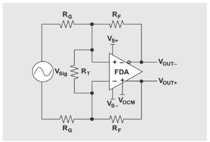
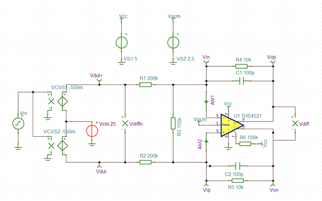
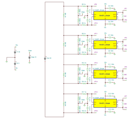
Rg is 20KOhm, Rf is 4.99KOhm and Rt for this specific test is not present, I have however a different setup with Rt of 12.9KOhm which presents the same issue. My ADS1278 follow the same schematic concept as in the reference board with an OPA2350 for the VCOM output to the THS4521. The ADS1278 acquires 8 differential signals, each one buffered by a THS4521 and it is configured in High-Speed mode and acquiring in this specific case 100KSPS. The voltages fit and the channels, if its negative input is connected to the ground, are very accurate. The ADS1278 is interfacing with a Microcontroller in an isolated way and has its own isolated supply. All values are transferred to a computer via ethernet and read in a Labview application.

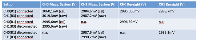
Now to the test, if I connect just one differential channel to the setup above, for instance to R1, the voltage measured is very accurate (compared to a Keysight 34470 multimeter). If I connect one channel to R1 and another channel to R3 for instance then problems happen. The Vr1 increases in up to 60mV, which is a killer for my application. Due to the input impedance of the THS4521 (in my setup arround 60KOhm), an increase of 1mV could be reasonable when connecting 2 channels, but not up to 60mV. See a table below with a part of the measurements that I have performed:

It might very well be, that I have not well understood the principle of differential measurements, but this is really a killer for my application. I would really appreciate inputs to solve this or to get to the root cause. Worst case I would have to change the whole concept, but I hope I can solve this issue somehow.

Thanks and Best Regards,

Javier

  • Hello Javier,

    Based on your accuracy requirements, I do not think this approach will work.  The differential input impedance in this case is 2*Rg=40kOhm, but the common mode input impedance is approximately (Rg+Rf)/2=12.5kOhm.  This common mode impedance will have additional current relative to the common mode voltage.

    In your above example, I assume the debugging setup is isolated from the power supply used for the ADS1278.  (There is no ground connection between the 15V source and the ground of the ADS1278.)  In this case, if you only connect one channel, then the only error will be due to the input differential impedance of that channel, or 40kOhm in parallel with your 100ohm resistor.  However, once you connect a second channel, you now have a common mode path between the channels and the ADS1278 ground.  In this case, much more current will flow.  I would need to setup a SPICE simulation to get exact numbers, but I think if you connected an input channel to R1 and a second channel to R5, you will now see an approximate common mode current of 15V/(CH1CM_Rin+CH2-CM_Rin)=0.6mA.  0.6mA of error current through the 100ohm resistor will result in about 60mV of error voltage.

    If you are measuring across a much lower impedance source, such as a string of batteries, then the error voltage will reduce quite a bit.  You can verify this by using 10Ohm resistors (will need to be higher power rating) instead of the 100ohm resistors and do the same tests.

    If you are measuring voltages on a resistor network similar to your setup, you will need to use either a difference amplifier with a much higher input impedance, or for best performance, an instrumentation amplifier.  Unfortunately, with the THS4521, you really cannot increase the resistor values higher than what you already have and maintain good DC (input bias currents will create additional errors) and AC performance (input capacitance will interact with the feedback resistance, causing stability issues).

    Assuming your common mode voltage is in the range of +/-10V, and you have +/-15V supplies available, you could use the INA851.  This is a differential output instrumentation amplifier that can directly drive the ADS1278 inputs, removing the need for the THS4521.

    Another possible option is to use the INA149.  This is a difference amplifier that supports much higher common mode voltages, and uses much higher input resistors.  The resulting error current will be much lower than the configuration you created with the THS4521.  If using the INA149, you will need to also use the THS4521, since the output stage of the INA149 will not be able to drive the ADS1278 input and maintain high accuracy.  Also, the INA149 can operate from a single 5V supply, but the output will be limited from 1.5V to 3.5V in this case, which will limit the input difference voltage as well.

    If you can provide additional details on what you are actually trying to measure (source impedance, common mode voltage range, differential voltage range), I can refine my recommendations.

    Regards,
    Keith Nicholas
    Precision ADC Applications

  • Hello Keith,

    fist of all thanks a lot for your time and ideas, by reading it I realize why I like to use parts from TI. I have yet to see another forum where I can get such a level of support. Regarding my application, it is basically meant for measuring voltage drops among semiconductors (typically Vds in SiC MOSFETS, Vce in IGBTs or Vf in Diodes) which are placed in series in several branches which are connected in parallel (up to 4) and each one enabled/disabled via a switch (MOSFET) for a certain period of time. It is basically power cycling:

    Below I1, I2 and I3 we would have up to 4 devices under test connected in series. We have as well applications where the target would be to measure leakage currents from semiconductors. Precisely to the requirements actually for each DUT, depending on the test:

    1- We would have to be capable of reading signals with 10Vpp differentially for each channel (DUT), for a complete branch the requirement would be in worst case 45Vpp (we could limit it to 40Vpp if necessary). In our measurement system we have several isolated ADC blocks with ADS1278 but it would be important to be able to cover one complete branch with just one block. This would mean, that between channels of the same ADS1278 the voltage difference could get up to almost 45Vpp (common mode voltage range).

    2- Regarding input impedance of each channel, ideally we shall be able to increase it to >1Gohm, although here we have some flexibility if we have to balance among requirements.

    3- Regarding the supply of the front-end, it would be important that we manage to use the single supplies of the ADS1278, f.i. the 5V one, as it is the case currently for the THS4521. Regarding the voltage we have some flexibility though (if really necessary), as before the LDOs that supply the ADS1278 we have a flyback with output voltages of around 8V, but I could increase them easily and place an additional LDO if necessary. The important thing is to cope with 1 single supply if feasible to reduce complexity.

    4- Regarding the package, the VQFN of the INA851 would be an issue. We would like a package which is more hand-soldering friendly for rework/development, such as the SOIC or VSSOP.

    5- If possible I would as well try to avoid using a combination of two amplifiers, such as THS4521 and INA149, but a single one.

    6- As we will have to use many amplifiers for each board, the BoM costs shall be optimized as much as possible (f.i. INA826 or INA821?). If we can find some parts which are cost effective we could leverage some of the requirements.

    Given these requirements what would you think it would be the most suitable TI part?

    Another question. Do you think that there is a way to increase the input impedance (common and differential) of the THS4521 at the expense of noise so that we come from the 60mV difference of the setup that I have sent to you to something in the area of 1mV? The question here is really if we can fix short term somehow these first boards to run some tests.

    Thanks again for your valuable support,

    Javier

  • Hello Javier,

    You may be able to increase the input resistors to 400k; according to simulations it looks like this should work.  However, in order to support up to 45Vpp of common mode, you will need to increase the attenuation (reduce the gain).  This will reduce the differential voltage at the ADC inputs, resulting in lower SNR, but this may still be acceptable.  In any case, with such a high common mode voltage, in order to reduce common mode errors, the tolerance for the resistor networks will need to be 0.05% or lower.

    Below is a suggested circuit to try out.  The offset voltage will increase as Rf increases due to the mismatch in input bias currents, but you should be able to calibrate this error.

    If you need 1Gohm input resistance, then the only way to achieve this is to use high-voltage input buffers, which will require a supply voltage greater than the common mode input voltage.

    Since you need to support common mode voltages up to 45V, the instrumentation amplifiers are not going to work.  In this case, creating a discrete solution using the THS4521 is probably your best choice.

    Regards,
    Keith

  • Hello Keith,

    thanks, I will follow your advice and try the modifications on the THS4521 circuit. Regarding the 45Vpp, the majority of our applications would just need 20Vpp. Would an INA821 or an INA826 fit in this case?, which supply would we need for them?

    Would it be possible that show me the reworked THS4521 setup for the 20Vpp as well? How do you calculate the maximum input common mode voltage of the THS4521 and the related attenuation factor to comply with it?

    Regards,

    Javier

  • Hello Arijav,

    My below comments are based on the assumption that the ADS1278 board ground can be connected to the low side of the DUT, as shown in the figure below (required for proper INA82x input bias).  Also, I assume the voltage on the DUT relative to this system ground will aways be positive.

    In this case, you could use the INA826 with a single supply that is 1V or more greater than the maximum input common mode that needs to be measured.  If the maximum voltage on the top side of the DUT (emitter of the IGBT) is 20V, then the supply voltage for the INA826 would need to be 21V or higher (up to the maximum rated voltage of 36V).

    In this configuration, the INA826 would be able to measure a differential voltage from 0.1V up to 10V.  If the INA826 was powered with the maximum 36V rating, then it could support measurements up to 35V on the top side of the DUT (emitter of the IGBT) relative to the ground shown above.

    I ran a SPICE simulation to determine the minimum attenuation needed to meet the input voltage requirements of the THS4521.  Re-running the simulation with a maximum voltage of +20V results in a gain of 2x the previous recommendation, or Gain=0.05.  Your initial design, with Gain=0.25, common mode is limited to about +7.5V.

    Regards,
    Keith

  • Dear Keith,

    I have setup in Tina the same simulation that you have prepared and now I understand better how to tune the current circuit based on the THS4521 for my needs, many thanks.

    For the next revision I am still wondering which is the best path. I have 2 options considering a maximum Common Mode voltage of 25Vpp:

    1- INA149 + THS4521: In this case I might have to go to 2 rail supplies but it could be a good solution. Is there any application note where I can see a design both with the INA149 as well as the THS4521 with an ADC? In this case I would use the THS4521 with a gain of 1, correct?

    2- INA821/826: Actually in my application I do not have a ground connection from the ADS1278 block as you have shown in your picture. I would prefer as well to avoid it if it is not 100% necessary. If I understand you well this is a must have for these instrumentation amplifiers, correct? Are there as well application notes where I could see the design for an INA821 together with an ADC? Specifically for the INA821 I will run some simulations but I have already used your Analog Engineering Calculator:

    If I do not connect the Grounds my assumption would be that I would be able to have input common mode voltage differences of up to 20Vpp for +/-18V supplies. This would be even if not perfect quite good for many of my applications. Is it really necessary to connect the grounds?

    Thanks and Regards,

    Javier

  • Hello Javier,

    I am not aware of any specific application notes that show the combination of the INA149 and a differential amplifier.  However, the INA149 is a fixed gain of one, so you would still need to attenuate by 4x for a 10V differential input when using the ADS1278 with a reference of 2.5V.

    Here is an application note that shows using the INA149 with a +/-10V ADC input.  Using the THS4521 with a gain of 0.25 will then provide the same input signal range.

    https://www.ti.com/lit/an/sbaa337/sbaa337.pdf

    Regarding the use of an instrumentation amplifier, you can use one of these devices without a direct ground connection to the DUT, but you need to use biasing resistors in the 1Meg to 10Meg range.  The below application note discusses this approach.

    https://www.ti.com/lit/an/sboa503/sboa503.pdf

    If interested in more background information, we have a training series, TI Precision Labs, with a lot of material.  There is an entire section that covers the use of Instrumentation amplifiers.

    https://www.ti.com/video/series/precision-labs/ti-precision-labs-instrumentation-amplifiers.html

    Regards,
    Keith

  • Thanks Keith, one last question. When using the INA821 I will have to attenuate the signal with a 0.25 factor. Do I have to use the THS4521 additionally to the INA821 or is there a more effective way to do so?

    Due to the topic of the attenuation I am actually rethinking the use of the INA851, even if it is not that cost effective.

  • Hello Javier,

    In the case of the INA821, the minimum differential gain is 1, so for a 10V differential input, you will need an additional attenuation of 0.25.  The most convenient place to do this is in the THS4521 stage.

    One other possibility; since you need a differential gain less than 1, another option is to use a PGA.  The PGA855 can be set to a gain of 0.25, and can directly drive the ADS1278 inputs using the differential output.  However, similar to the INA851, this part is only available in a QFN package.

    Regards,
    Keith

  • Thanks Keith, I have decided however to move forward with the INA851. Would you suggest me to use for each channel of the ADS1278 the same circuit as in figure 9-9 of the datasheet and adding the 1 to 10M biasing resistors between Vin- and GND and Vin+ and GND or shall I modify something? My target is to sample the channels at 100KSPS:

    The VOCM pin for the 8x INA851 can be driven in the same way as with the THS4521 using an OPS2350 and the VCOM output of the ADS1278, right? In my current design I have a 100K resistor and a 100nF capacitor instead of the 10Ohm and 150pF shown in the datasheet.

    I have as well modified the current design with the THS4521 using 200k + 10k Resistors. Unfortunately I experience exactly the same behavior as before. If I read the voltage of R1 when R5 is connected the voltage jumps around 180mV this time (probably more than before because of the attenuation factor). Therefore this issue at least for the THS4521 does not have to a relationship with the resilience to higher common mode voltages. Do you have any clue what could be the root cause for it?, I would not like to go to a new design with the INA851 and realize that I have still the same issue...

    Regards,

    Javier

  • Hello Javier,

    Yes, I would use the values in Figure 9-9 between the INA851 outputs and the ADC inputs.

    For the inputs, in addition to the 1M to 10M input bias resistors, I suggest adding a differential input noise filter.  You may not need these components, but if there is a lot of RF/EMI noise that is picked up on the input connections, the addition of this filter will be very helpful to reduce measurement noise.  Please refer to the EVM user's guide for the INA851 for more details, including suggested board layout.

    Regarding the VCOM pin, yes, you can use the same approach as used with the THS4521.  Buffer the common mode output of the ADS1278 and drive the 8 VOCM input pins of the INA851 devices.

    Changing the THS4521 feedback resistors to 200k and 10k should reduce the effects between channels.  I am not sure what is going on in this case.  I would suggest using a hand held DMM to measure the inputs with equivalent resistor networks added to each of the measurement channels.  This should help debug the root cause.

    Regards,
    Keith

  • Thanks Keith. Regarding the THS4521, I have now replaced not just the resistors but the ICs themselves by brand new ones bought at Mouser and I see now differences of 2-3mV in spot checks. I have bought the old THS4521 during the time where there was no stock anywhere from a Chinese reseller, maybe they were counterfeits. I am using the setup of 400K + 10K resistors to maximize the robustness against common mode input voltage. I will perform more intensive tests but for the time being I think I will be able to use the boards that were manufactured. The next ones will come with the INA851 for sure.

  • Hello Javier,

    Thanks for the update.  If the THS4521 is hard to locate, you can also use the newer version of this amplifier; THS4551.

    Regards,
    Keith

  • Hello Keith,

    thanks again for your input. 3 last (I think :) ) questions:

    1- Do you think with the THS4551 I would be able to reduce even further the issue of the common mode voltage (I am now at 2-3mV diff.)

    2- Do I need for my setup as well biasing 1M to 10M resistors with the THS4521 (or THS4551)?

    3- Is the INA851 really going to improve my problem, which is mainly the influence of the input common mode voltage in the output differential voltage? It seems it does not have a higher CMRR with an output gain of 0.2 as the THS4521 or THS4551.

    Regards,

    Javier

  • Hello Javier,

    1 - The THS4551 has better DC specifications, so using this part should help with overall system accuracy.  However, the common mode rejection is primarily determined by the feedback resistor matching.  0.1% tolerance resistors will result in about 60dB of common mode.  This means a 10V common mode level will result in 10mV of differential voltage, in addition to all other errors.  If you need to reduce this error further, you will need better than 0.05% tolerance resistors.  A possible solution would be to use a matched resistor network, assuming the correct values are available.

    2 - If only using a THS4521 or THS4551, then no additional biasing resistors are required in this case.  The feedback resistors provided the necessary biasing current required by the amplifier.

    3 - INA851 in a gain of 0.2 has a minimum common mode rejection of 76dB.  This is equivalent to using feedback resistors with 0.01% tolerance.  It is roughly 10x better than what you can get using the THS4551 (THS4521) with 0.1% tolerance resistors.  However, the additional improvement is the high input impedance of the INA851.  This will be reduced since you need to add biasing resistors, but you will still be in the 1MOhm range.

    Regards,
    Keith

  • Thanks a lot Keith for the detailed answer. I have just one last question (this time for sure :) ). Neither the 1M biasing resistors on the INA851 nor the input filter are not going to reduce further the CMRR of 76dB (Min.), right?

  • Hello Javier,

    I looked at your setup in a little more detail.  The preferred way to bias the system is to use a single 1MEG resistor connected to the lowest voltage potential in the resistor network.  Assuming you want to use a single supply for the instrumentation amplifier, then you should bias the point to the ADC reference, or 2.5V.

    This configuration will then establish a proper bias voltage point for all input channels since you are DC coupled to each DUT.  The below diagram shows the suggested configuration.

    The INA blocks are ideal instrumentation amplifiers, with the input bias current of the INA851 modeled.  There are slight differences, and this is due to the bias currents and the DUT impedance.  However, you can see with DUT impedances up to 10kOhm, the errors are less than 1mV (about 300uV in this case).  So yes, there is still some effect on CMRR, but this depends on the DUT impedance and total common mode voltage.  This is in addition to the INA851 CMRR spec.  However, with this setup, you should be able to get accurate measurements with less than 1mV error.

    Regards,
    Keith

  • Hello Keith,

    thanks for the new bias proposal. Unfortunately in my setup this would be quite difficult to implement, as the operators of the tests would always have to check with care which is the DUT which is closer to ground and therefore connect the channel with the bias resistor to it. I am certain that mistakes will be made.

    Which error could I expect with the original setup of the 2x1MOhm (0.1%) resistors per channel connected to the ADC ground and up to 20V common mode voltage difference at the inputs?

    Best Regards,

    Javier

  • Hello Javier,

    I will respond later today or tomorrow.

    Regards,
    Keith

  • Hello Javier,

    The error will depend on the resistance of each DUT.  Total error should be 1mV or less when using 10MOhm bias resistors on each channel, and maximum DUT resistance of 1kOhm.  If bias resistors are 1MOhm, then maximum DUT resistance will be 100Ohm.

    Having multiple bias points shifts the bias voltage, making it dependent on the total DUT voltage, as well as the supply voltage.  Below is a use case where the INA851 is powered from a single 36V supply.  The bias voltage in this case is set to 13.75V, which will allow the DUT voltage to range up to 30V and still meet the input voltage requirements of the INA851.

    I am going to be out of office after tomorrow for the remainder of the year and will not be able to respond to any more e2e posts until Jan 2nd.

    Regards,
    Keith

  • Hello Keith,

    first of all I wish you a Happy New Year. I'm still wondering which is the best biasing solution in my precise case. In my case the DUTs are actually connected to a current source which has typically a maximum voltage of 15V to 20V. The current is however regulated and therefore, depending on the number of the DUTs in a branch and other constraints such as its Rdson the voltage could really go way below those 15V to 20V. The current itself for each branch can range from 10mA (provided by a different measurement current source), 100A and up to 2000A depending on the precise testbench and testing step. Does it makes sense therefore to have a constant bias of 13.75V as you propose in your last example or to have a kind of floating bias which will be settled once the DUTs are all connected and depending on the working point? (the initial idea of the two 10M biasing resistors for each INA851 to the Common Ground of the ADC). In case of the original option I am as well wondering if there is a benefit on adding a 3rd resistor (1M) between the +/- Inputs of the INA851 as shown in the SBOA503 application (page 7) to reduce the input common mode influence.

    Regards,

    Javier

  • Hi Arijav,

    We need additional time to respond to this question, please expect a response in approximately 1 week. Thanks for your patience

    -Bryan

  • Hi Bryan,

    thanks for your feedback. I will patiently wait for the response then.

    Best Regards,

    Javier

  • Hi Arijav,

    We were unable to get to this question this week, we hope to have a response back to you by Wednesday next week because Monday is a holiday

    -Bryan

  • Hello Javier,

    Yes, after taking a break from looking at this unique setup, I think I agree.  Simply using 1M for each INA input to a common mode voltage that is the midpoint of the INA supplies is probably going to work the best.

    I need to point out that you will need a bipolar supply for the INA851 in order to cover a wide range of inputs.  The proposed circuit supports a total DUT voltage up to 30V using INA851, but the supplies required for the INA851 to cover this full input range are VS-=-3V and VS+=33V, with the bias voltage set to midpoint of 15V.

    Zoomed in version:

    This setup assumes that the supply voltage of the INA851+ADS1274 is either isolated from the DUT source, or, the DUT has a common ground on the negative side, as suggested earlier in this e2e thread.

    Using instrumentation amplifiers or difference amplifiers typically assumes there is a common ground between the DUT and the measurement system.  In industrial systems, this is usually EARTH ground.  In your case, you have a floating DUT relative to your measurement system, which is why this approach is complex to analyze.

    Regards,
    Keith

  • Hello Keith,

    Thanks for the detailed answer. What I am doing currently in the design is actually via an isolated Flyback to generate from the main Supply +18V and -18V. I use those voltages to supply the INAs of an ADS1278 block. The ADS1278 5V,3.3V and 1.8V supplies are generated via another non-isolated Flyback that is attached to the Ground of the first isolated Flyback and its +18V supply and 3xLDOs attached to its output. The VCOM input from the INAs (in total 8x per Block) go to the 2.5V Output of the ADS1278 buffered by an OPA2350. Do you see any inconvenience in this case?

    My filtering seems slightly different as in your last example (I followed the suggestion on one of your first posts). Do you think it is better to use your last suggestion?

    I had as well a question related to the SBOA503 (Page 7). It seems there instead of 1MOhm resistors 10MOhm resistors are used to INA ground and additionally a 3rd 1MOhm resistor between the INA inputs. Does it make sense in my application or would you leave the design as per your last suggestion?

    Regards,

    Javier

  • Hello Javier,

    My previous reply is still a simplified schematic.  The configuration that you show above will work.  However, I recommend connecting the 1M (or 10M) resistors directly to the inputs (INA_AINN1 and INA_AINP1) to reduce any gain error. 

    Yes, you can also use 1M resistor differential and 10M for bias, as suggested in the application note to improve measurement accuracy (reduce offset). 

    Also, I would suggest reducing the capacitor values by 10x and increasing the resistor values by 10x to improve input-over voltage protection.  You have a TVS diode to protect the differential; you may also need a TVS to the system ground as well.

    Following all of these recommendations, the circuit will look like the below image:

    Also, as long as the entire measurement circuit operates off of an isolated power supply relative to your DUT (bipolar supplies for the INA851, 5V,3.3V,1.8V supplies for ADS1278), then you can use +/-18V supplies and the bias voltage will then simply be connected to the circuit ground.  This should allow a total voltage across 4 DUTs of about 28V and still meet all of the input and output voltage requirements of each INA851.

    The VCOM input from the INAs (in total 8x per Block) go to the 2.5V Output of the ADS1278 buffered by an OPA2350. Do you see any inconvenience in this case? 

    Yes, using OPA2350 to buffer the VCOM signal and then routing to each INA851 should work well.

    Regards,
    Keith

  • Hello Keith,

    thanks a lot for your answer, I will follow your recommendations!

    Regards,

    Javier

  • You are Welcome!