This thread has been locked.

If you have a related question, please click the "Ask a related question" button in the top right corner. The newly created question will be automatically linked to this question.

ADS1248EVM-PDK: ADS1248EVM Web App constantly reports EVM board is not present

Part Number: ADS1248EVM-PDK
Other Parts Discussed in Thread: ADS1248

Main Issue: I removed/inserted the USB cable attached to the ADS1248EVM board a few times, and the browser plugin indicator appears to detect the ADS1248EVM board because it illuminates to RED, but repeatedly reports “DEVICE DISCONNECTED”.

Here are the driver files that i have loaded, please advise if these are correct.
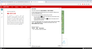
 

  • Here is the Windows driver that I am using for the ADS1248EVM board.

    https://www.ti.com/tool/download/SBAC253

    Does this driver support Windows 11 ?

    I am using the latest Chrome Web Browser, what settings should Chrome enable for the 

    ADS1X48EVM-PDK-GUI browser plugin, located at:

    https://dev.ti.com/gallery/view/PADC/ADS1x48EVM_GUI 

    to work properly ?

  • Hi Tim,

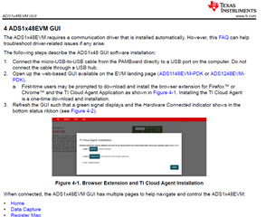
    Can you show the GUI page after you close the README?  If there is a driver issue, there should be another popup box explaining why the GUI cannot connect.  The drivers should automatically install.  It appears that you have the bulk driver, but the EVM also enumerates as CDC as well.  So in device manager there should be both USB Bulk and a COM port assigned to the EVM.  Both of these drivers are actually native to the MS-OS and should install automatically.  But using the download should also assign them correctly.

    For the EVM, make sure that both boards are correctly oriented together.  On the bottom board, do you see any lights illuminated and can you tell me which ones are lit (a picture would also help if you want to attach it)?

    Thanks,

    Bob B

  • Hello Bob and thanks for your reply.

    The README immediately pops up again, it basically just covers a GUI showing the image of a ADS card with some WebUI interface buttons from what I'm able to briefly see.  The USB Bulk and COM port are present in device manager and yes, the board is oriented correctly, it came like that out of the box from TI as compared to the .PDF pic and the specified LEDs (D1,D2: Top board). (D1,D5: bottom board) light up as stated in the .PDF.

  • Hi Tim,

    I'm sorry you are having issues.  If you click on 'don't show again', and then close the ReadMe what happens?  There might be some issue with the TICloud agent installation.  The issue appears to be more on the GUI side then the hardware side.  So I don't think it is a driver issue.

    Best regards,

    Bob B

  • I have everything working now. The problem was Admin rights! My IT department logged in and re-installed drivers with Admin rights. I am now able to detect the ADS1248 board, see registers, etc.

    Thanks again.

  • Hi Tim,

    I'm glad to hear you got things working.  I appreciate you sharing your resolve.

    Best regards,

    Bob B

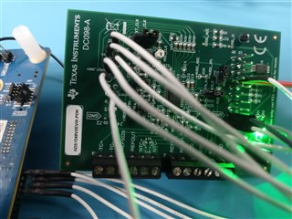
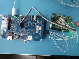
  • Question: Can the DC098-A board be removed from the DC081A board and be connected via SPI bus only to another board such as an STM32H735G-DK ?

    I have it (DC098-A) wired to an STM32H735G-DK but am not able to read back the ADS1248 default registers after RESET/POWER-ON.

    Thanks.

  • Hi Tim,

    Yes, you can disconnect the two boards and work with a different microcontroller.  Both DVDD and AVDD supplies must be at nominal voltage, the RESET pin pulled high and the START pin pulled high to read and write registers (see the note under Table 19 in the datasheet).

    Also, if you use CS this will need to stay low throughout the entire communications transaction.  If CS toggles between bytes the communication will cancel each time CS goes high.  Usually this will require that CS is controlled by GPIO.

    Best regards,

    Bob B

  • I re-checked everything, even set SCLK to 1MHz down from 2MHz. 'Im having difficulty with this,  as this chip works so easy with its own EVAL Motherboard. LoL. :-),  Is it possible that my wires are too long ?

    Thanks Again.

    Tim


  • Hi Tim,

    I would recommend setting the START pin high and seeing if the part is active by monitoring DRDY to see if the output is pulsing at the default data output rate.  If it is not, then you need to recheck your connections and primarily +5V, +3.3V, GND, RESET and START.

    If DRDY is pulsing, then the part is active.  It is possible that the wiring could be an issue, but I have seen a lot worse so you should be able to communicate.  With a scope check the signal integrity of SCLK, DIN and DOUT.  Make sure that the micro SPI out is on DIN and DOUT connects to the micro SPI in.

    If you still are having issues, please send me some oscilloscope or logic analyzer shots of the communication to help troubleshoot.

    Best regards,

    Bob B

  • +5V:     GOOD

    +3.3V:  GOOD

    GND:    GOOD

    RESET: HIGH

    START: HIGH

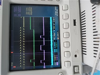
    SCLK and DRDY: (PULSES)

    SCLK and DIN:

    SCLK and DOUT_DRDY:

  • Hi Tim,

    I'm not clear on the scope shots.  Is there any way you can show at least DIN, DOUT and SCLK at the same time?  For this picture it looks like you labeled it as SCLK and DIN:

    So if it is DIN, the beginning of the command is incorrect as 0x80 is not a valid command.  So what would be most helpful is for you to show the complete communication and tell me what you are trying to send/receive.

    Best regards,

    Bob B

  • Hello Bob,

    A continued thanks for all of your support.

    Below is a short and simple test i wrote just to bring the ADS1248 out of RESET

    write to its registers to setup for an ADC conversion and read back a register value

    (MUX0) just to see if one of my Reg config settings were properly written.

    I will grab another scope probe and show SCLK, D_IN and D_OUT.

    Tim

    #define ADC1248_RREG_CMD 0x20

    #define ADC1248_WREG_CMD 0x40


    void RTD_Read_Reg ( uint8_t uRegNum, uint8_t uNumReg )

    {

    uint8_t ADC1248_CMD [ 15 + 2] = { 0 };

    uint8_t ADC1248_MISO [ 15 + 2 ];

    int n = 0, i =0;

    memset ( ADC1248_MISO, 0, sizeof(ADC1248_MISO));

    ADC1248_CMD [ 0 ] = ( ADC1248_RREG_CMD | uRegNum );

    ADC1248_CMD [ 1 ] = uNumReg;

    if (HAL_SPI_TransmitReceive(&hspi5, (uint8_t*)ADC1248_CMD, (uint8_t *)ADC1248_MISO, (uNumReg + 1), 5000) != HAL_OK )

    {

    Error_Handler();

    }

    HAL_Delay (10);

    }

    void RTD_Write_Reg ( uint8_t uRegNum, uint8_t uRegVal )

    {

    uint8_t ADC1248_CMD [ 15 + 2] = { 0 };

    uint8_t ADC1248_MISO [ 15 + 2 ];

    ADC1248_CMD [ 0 ] = ( ADC1248_WREG_CMD | uRegNum );

    ADC1248_CMD [ 1 ] = 0;

    ADC1248_CMD [ 2 ] = uRegVal;

    if (HAL_SPI_TransmitReceive(&hspi5, (uint8_t*)ADC1248_CMD, (uint8_t *)ADC1248_MISO, 3, 5000) != HAL_OK )

    {

    //debug_printf("ADS1248 RTD_Write_Reg failure!!!\r\n");

    //debug_printf("ADS1248 Stopped.\r\n");

    while (1);

    }

    HAL_Delay (10);

    //debug_printf("ADS1248 RTD_Write_Reg: %s, VAL: %.2xh\r\n",ads1248_reg_names[uRegNum], uRegVal);

    }

    int ADS1248_Init(void)

    {

    HAL_GPIO_WritePin(RTD_nRESET_GPIO_Port, RTD_nRESET_Pin, 0);

    HAL_Delay(60);

    HAL_GPIO_WritePin(RTD_nRESET_GPIO_Port, RTD_nRESET_Pin, 1);

    HAL_Delay(600);

    //debug_printf("ADS1248: Reset End\r\n");

    HAL_GPIO_WritePin(RTD_START_GPIO_Port, RTD_START_Pin, 1);

    HAL_GPIO_WritePin(RTD_nCS_GPIO_Port, RTD_nCS_Pin, 0);

    HAL_Delay( 600 );

    RTD_Write_Reg ( MUX0, (MUX_SP2_AIN2 | MUX_SN2_AIN3) );

    RTD_Write_Reg ( VBIAS, (VBIAS_3 | VBIAS_2) );

    RTD_Write_Reg ( MUX1, (REFSELT1_REF0 | MUXCAL2_REF0) );

    RTD_Write_Reg ( SYS0, (PGA2_0 | DOR3_1000) );

    RTD_Write_Reg ( OFC0, 0x01 );

    RTD_Write_Reg ( IDAC0, DRDY_PIN );

    RTD_Write_Reg ( IDAC1, 0xCC);

    RTD_Write_Reg ( GPIOCFG, CFG_ANALOG_INPUT_MODE );

    RTD_Write_Reg ( GPIODIR, 0 );

    RTD_Write_Reg ( GPIODAT, 0 );

    return 0;

    }

    int main(void)

    {

    ADS1248_Init();

    while (1)

    {

    RTD_Write_Reg ( MUX0, (MUX_SP2_AIN2 | MUX_SN2_AIN3) );

    RTD_Read_Reg ( MUX0, 1 );

    HAL_Delay (1000);

    }

        return 0;

    }

  • Hi Tim,

    It is difficult to tell from reading your code if there is an issue.  Scope shots of the communication is really the only way to verify.  I assume that HAL_Delay() is in milliseconds, correct?

    Best regards,

    Bob B

  • Hello and Good morning Bob,

    Yes, that is correct, HAL_Delay is in milliseconds. Still locating an additional probe or Logic Analyzer....

  • Hi Tim,

    At the very least can you set a breakpoint and capture the SCLK and DIN for a register write and tell me what you think should be happening at that point?

    Thanks,

    Bob B

  •    I'm just calling the init function to RESET the chip and set nRESET, nCS, START  to HIGH.

       Then write 0xFF to register MUX0. The breakpoint is set right after the  HAL_SPI_TransmitReceive in the RTD_Write_Reg function :

        if (HAL_SPI_TransmitReceive(&hspi5, (uint8_t*)ADC1248_CMD, (uint8_t *)ADC1248_MISO, 3, 5000) != HAL_OK )

       ADS1248_Init()

      {

    HAL_GPIO_WritePin(RTD_nRESET_GPIO_Port, RTD_nRESET_Pin, 0);

    HAL_Delay(60);

    HAL_GPIO_WritePin(RTD_nRESET_GPIO_Port, RTD_nRESET_Pin, 1);

    HAL_Delay(600);

    //debug_printf("ADS1248: Reset End\r\n");

    HAL_GPIO_WritePin(RTD_START_GPIO_Port, RTD_START_Pin, 1);

    HAL_GPIO_WritePin(RTD_nCS_GPIO_Port, RTD_nCS_Pin, 0);

       Return 0;

       }

    RTD_Write_Reg ( MUX0, 0xFF );

  • Hi Tim,

    Unfortunately I don't see all 24 SCLKs, but I can kind of guess from where the data starts.  A write register to MUX0 with FF requires the write register command (0x40 + register position (MUX0 = address 0x00)) + number of registers you wish to write less one (and one register is 0x00)  + data (0xFF).  So essentially it looks like this is what you are doing except the SPI DIN must be changing on the rising edge of SCLK and hold steady on the falling edge.  So you will need to change your PHASE setting for SCLK.

    Best regards,

    Bob B

  • In this screen-shot, i Init the ADS1248, then WReg 0xFF to MUX0 then RReg from MUX0. MUX0 should be 0xFF but what i see is random data every time. 

    [1] SCLK

    [4] D_IN

    [3] D_OUT

    ADS1248_Init();

    RTD_Write_Reg( MUX0, 0xFF );

    RTD_Read_Reg ( MUX0, 1 );

  • Ok, will do. 

    Thanks.

  • Hi Tim,

    It is not at all clear what this last scope shot is trying to show.  The SPI is full-duplex and it looks like you are writing and reading from the device.  The read register command (RREG) is similar to the WREG command in that there is two bytes for the command followed by the data.  So you would transmit 0x20 0x00 0xFF (which is NOP) to read the MUX0 register.

    Best regards,

    Bob B

  • I showed that i was writing 0xFF to MUX0 then reading it back. I put a breakpoint in the WReg() and RReg() functions in order to capture this.

    I never see the data buffer in RReg coming back with 0xFF, its either 0x00 or 0x33 or 0x80.

    So yes, i have my defines as:

    #define ADC1248_RDTA_CMD ( 0x12 )

    #define ADC1248_RREG_CMD ( 0x20 )

    #define ADC1248_WREG_CMD ( 0x40 )

    #define ADC1248_NOPR_CMD ( 0xFF )

    and the code is:

    RTD_Write_Reg ( MUX0, 0xFF );

    RTD_Read_Reg ( MUX0, 1 );

    SPI Settings:

  • Hi Tim,

    That is your code information.  Interpret for me the 16 SCLKs you showed in your last scope shot.  Either the RREG or WREG command requires 24 SCLKs.  The last thing you send to the ADS1248 is not a NOP.  The ADS1248 doesn't know any better than I do what you are trying to tell it. Slight smile

    Have you changed the phase to the correct value and capture the scope shot again?

    Best regards,

    Bob B

  • The 16 SCLKs are controlled by the STM32H HAL SPI functions whenever i do a Transmit/Receive.

    I wasn't trying to send a NOP, just Write 0xFF to MUX0 and read it back. 

    The ADS expects the SCLK phase settings to be:

    CPOL:  LOW

    CPHA: 1 Edge

    correct ?

  • Hi Tim,

    You would have to check the datasheet for the processor to know whether CPHA should be 0 or 1.  As it is currently wrong on the scope shots and you are using 1 then it must be 0 instead.

    As far as the communication is concerned, you must be sending the peripheral the wrong data in the transmit/receive function.  Regardless of whether you use the RREG or the WREG command there should always be 24 SCLKs.  The first two bytes are the command and the last byte is data.  So the data should be 3 bytes transmitted always.  This means for the RREG command you need to send the two command bytes (0x20 0x00) and a NOP (0xFF).  As you are not sending the NOP, the last byte of SCLKs are never sent (resulting in 16 instead of 24 SCLKs).  Internally, writing to the transmit buffer initiates the SCLKs.

    For the register data the contents will be in the 3rd byte of your array ADC1248_MISO[].

    After reviewing your code again I think I see the issue.

    void RTD_Read_Reg ( uint8_t uRegNum, uint8_t uNumReg )
    
    
    {
    
    
     uint8_t ADC1248_CMD [ 15 + 2] = { 0 };
    
    
     uint8_t ADC1248_MISO [ 15 + 2 ];
    
    
     int n = 0, i =0;


     memset ( ADC1248_MISO, 0, sizeof(ADC1248_MISO));
    
    
     ADC1248_CMD [ 0 ] = ( ADC1248_RREG_CMD | uRegNum );  // this is ok
    
    
     ADC1248_CMD [ 1 ] = uNumReg;  // This should be number of registers less 1 so when reading 1 register it shoudl be 0
     
     // you also need to send the NOP
     ADC1248_CMD [ 2 ] = 0xFF;
     // If uNumReg value is requesting more than one byte of data then you need to send additional NOPs
     // For example, the RDATA command to read back conversion results is the command and three bytes of data for a total of 4 bytes transmitted


     // The following is incorrect for the number of bytes as you are giving uNumReg + 1
     // If the uNumReg = 1, then for reading back 1 register you need to add 2 so that 3 bytes are sent (2 command bytes + NOP)
     if (HAL_SPI_TransmitReceive(&hspi5, (uint8_t*)ADC1248_CMD, (uint8_t *)ADC1248_MISO, (uNumReg + 1), 5000) != HAL_OK )
    
    
     {
    
    
     Error_Handler();
    
    
     }
    
    
     HAL_Delay (10);


    }


    Best regards,

    Bob B

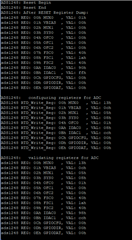
  • Thanks for all your help Again Bob, I finally got this working after paying attention to detail.

  • Hi Tim,

    Congratulations!  Always a nice feeling when things start to work.

    Best regards,

    Bob B